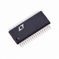
LTC1603IG#TR Linear Technology, LTC1603IG#TR Datasheet - Page 11

LTC1603IG#TR
Manufacturer Part Number
LTC1603IG#TR
Description
IC CONV A/D 16BIT 250KSPS 36SSOP
Manufacturer
Linear Technology
Datasheet
1.LTC1603CGPBF.pdf
(20 pages)
Specifications of LTC1603IG#TR
Number Of Bits
16
Sampling Rate (per Second)
250k
Data Interface
Parallel
Number Of Converters
1
Power Dissipation (max)
350mW
Voltage Supply Source
Analog and Digital, Dual ±
Operating Temperature
-40°C ~ 85°C
Mounting Type
Surface Mount
Package / Case
36-SSOP (0.200", 5.30mm Width)
Lead Free Status / RoHS Status
Contains lead / RoHS non-compliant
Available stocks
Company
Part Number
Manufacturer
Quantity
Price
APPLICATIONS
three-state until read by the MPU with the RD signal. Mode
2 can be used for operation with a shared data bus.
In slow memory and ROM modes (Figures 8 and 9) CS is
tied low and CONVST and RD are tied together. The MPU
starts the conversion and reads the output with the com-
bined CONVST-RD signal. Conversions are started by the
MPU or DSP (no external sample clock is needed).
In slow memory mode the processor applies a logic low to
RD (= CONVST), starting the conversion. BUSY goes low,
forcing the processor into a wait state. The previous
conversion result appears on the data outputs. When the
conversion is complete, the new conversion results
appear on the data outputs; BUSY goes high, releasing the
processor and the processor takes RD (= CONVST) back
high and reads the new conversion data.
In ROM mode, the processor takes RD (= CONVST) low,
starting a conversion and reading the previous conversion
result. After the conversion is complete, the processor can
read the new result and initiate another conversion.
RD = CONVST
RD = CONVST
CS = 0
BUSY
DATA
U
CS = 0
BUSY
DATA
INFORMATION
U
t
6
t
10
t
6
t
W
10
DATA (N – 1)
D5 TO D0
t
Figure 8. Mode 2. Slow Memory Mode Timing
CONV
DATA (N – 1)
D15 TO D0
t
CONV
t
11
U
Figure 9. ROM Mode Timing
t
7
D15 TO D0
DATA N
t
11
t
DIFFERENTIAL ANALOG INPUTS
Driving the Analog Inputs
The differential analog inputs of the LTC1603 are easy to
drive. The inputs may be driven differentially or as a single-
ended input (i.e., the A
A
wanted signal that is common mode to both inputs will be
reduced by the common mode rejection of the sample-
and-hold circuit. The inputs draw only one small current
spike while charging the sample-and-hold capacitors at
the end of conversion. During conversion the analog
inputs draw only a small leakage current. If the source
impedance of the driving circuit is low, then the LTC1603
inputs can be driven directly. As source impedance in-
creases so will acquisition time (see Figure 10). For
minimum acquisition time with high source impedance, a
buffer amplifier should be used. The only requirement is
that the amplifier driving the analog input(s) must settle
after the small current spike before the next conversion
8
t
8
IN
–
inputs are sampled at the same instant. Any un-
D15 TO D0
DATA N
D15 TO D0
DATA N
IN
–
input is grounded). The A
DATA (N + 1)
D15 TO D0
1603 F09
LTC1603
1603 F08
11
IN
+
and
1603f


