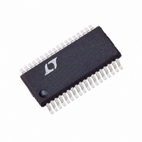
LTC1603IG#TR Linear Technology, LTC1603IG#TR Datasheet - Page 13

LTC1603IG#TR
Manufacturer Part Number
LTC1603IG#TR
Description
IC CONV A/D 16BIT 250KSPS 36SSOP
Manufacturer
Linear Technology
Datasheet
1.LTC1603CGPBF.pdf
(20 pages)
Specifications of LTC1603IG#TR
Number Of Bits
16
Sampling Rate (per Second)
250k
Data Interface
Parallel
Number Of Converters
1
Power Dissipation (max)
350mW
Voltage Supply Source
Analog and Digital, Dual ±
Operating Temperature
-40°C ~ 85°C
Mounting Type
Surface Mount
Package / Case
36-SSOP (0.200", 5.30mm Width)
Lead Free Status / RoHS Status
Contains lead / RoHS non-compliant
Available stocks
Company
Part Number
Manufacturer
Quantity
Price
Input Range
The 2.5V input range of the LTC1603 is optimized for low
noise and low distortion. Most op amps also perform well
over this same range, allowing direct coupling to the
analog inputs and eliminating the need for special transla-
tion circuitry.
Some applications may require other input ranges. The
LTC1603 differential inputs and reference circuitry can
accommodate other input ranges often with little or no
additional circuitry. The following sections describe the
reference and input circuitry and how they affect the input
range.
Internal Reference
The LTC1603 has an on-chip, temperature compensated,
curvature corrected, bandgap reference that is factory
trimmed to 2.500V. It is connected internally to a refer-
ence amplifier and is available at V
12a). A 7.5k resistor is in series with the output so that it
can be easily overdriven by an external reference or other
circuitry (see Figure 12b). The reference amplifier gains
the voltage at the V
internal reference voltage. This provides buffering
between the V
The reference amplifier compensation pin (REFCOMP,
Pin 4) must be bypassed with a capacitor to ground. The
reference amplifier is stable with capacitors of 22 F or
greater. For the best noise performance a 47 F ceramic
or 47 F tantalum in parallel with a 0.1 F ceramic is
recommended.
APPLICATIONS
ANALOG INPUT
REF
Figure 11. RC Input Filter
pin and the high speed capacitive DAC.
3000pF
REF
U
100
47 F
pin by 1.75 to create the required
INFORMATION
U
1
2
3
4
5
A
A
V
REFCOMP
AGND
REF
IN
IN
REF
W
+
–
LTC1603
(Pin 3) (see Figure
1603 F11
U
The V
shown in Figure 13. This is useful in applications where the
peak input signal amplitude may vary. The input span of
the ADC can then be adjusted to match the peak input
signal, maximizing the signal-to-noise ratio. The filtering
of the internal LTC1603 reference amplifier will limit
the bandwidth and settling time of this circuit. A settling
time of 20ms should be allowed for after a reference
adjustment.
Differential Inputs
The LTC1603 has a unique differential sample-and-hold
circuit that allows rail-to-rail inputs. The ADC will always
convert the difference of A
common mode voltage (see Figure 15a). The common
mode rejection holds up to extremely high frequencies
(see Figure 14a). The only requirement is that both inputs
Figure 12b. Using the LT1019-2.5 as an External Reference
4.375V
REF
2.500V
LT1019A-2.5
pin can be driven with a DAC or other means
47 F
Figure 12a. LTC1603 Reference Circuit
V
5V
IN
3
4
5
V
V
REFCOMP
AGND
OUT
REF
+
10 F
ANALOG
INPUT
16k
R3
IN
REFERENCE
12k
+
R2
0.1 F
AMP
– A
1
2
3
4
5
IN
A
A
V
REFCOMP
AGND
IN
IN
REF
–
+
–
LTC1603
independent of the
7.5k
R1
LTC1603
REFERENCE
1603 F12b
BANDGAP
LTC1603
1603 F12a
13
1603f


