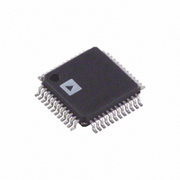
AD9218BSTZ-105 Analog Devices Inc, AD9218BSTZ-105 Datasheet - Page 19

AD9218BSTZ-105
Manufacturer Part Number
AD9218BSTZ-105
Description
IC ADC 10BIT DUAL 105MSPS 48LQFP
Manufacturer
Analog Devices Inc
Datasheet
1.AD9218BSTZ-40.pdf
(28 pages)
Specifications of AD9218BSTZ-105
Data Interface
Parallel
Number Of Bits
10
Sampling Rate (per Second)
105M
Number Of Converters
2
Power Dissipation (max)
565mW
Voltage Supply Source
Analog and Digital
Operating Temperature
-40°C ~ 85°C
Mounting Type
Surface Mount
Package / Case
48-LQFP
Resolution (bits)
10bit
Sampling Rate
105MSPS
Input Channel Type
Differential
Supply Voltage Range - Analog
2.7V To 3.6V
Lead Free Status / RoHS Status
Lead free / RoHS Compliant
Available stocks
Company
Part Number
Manufacturer
Quantity
Price
Company:
Part Number:
AD9218BSTZ-105
Manufacturer:
ADI
Quantity:
455
Company:
Part Number:
AD9218BSTZ-105
Manufacturer:
Analog Devices Inc
Quantity:
10 000
Part Number:
AD9218BSTZ-105
Manufacturer:
ADI/亚德诺
Quantity:
20 000
VOLTAGE REFERENCE
A stable and accurate 1.25 V voltage reference is built into the
AD9218 (VREF OUT). Typically, the internal reference is used
by strapping Pin 5 (REF
(REF
independently by varying the reference voltage inputs applied to
the AD9218. No appreciable degradation in performance
occurs when the reference is adjusted ±5%. The full-scale range
of the ADC tracks reference voltage, which changes linearly
(a 5% change in VREF results in a 5% change in full scale).
TIMING
The AD9218 provides latched data outputs, with five pipeline
delays. Data outputs are available one propagation delay (t
after the rising edge of the encode command (see Figure 2
through Figure 4). The length of the output data lines and loads
placed on them should be minimized to reduce transients
within the AD9218. These transients can detract from the
dynamic performance of the converter.
The minimum guaranteed conversion rate is 20 MSPS. At clock
rates below 20 MSPS, dynamic performance degrades.
USER SELECT OPTIONS
Two pins are available for a combination of operational modes,
enabling the user to power down both channels, excluding the
reference, or just the B channel. Both modes place the output
buffers in a high impedance state. Recovery from a power-down
state is accomplished in 10 clock cycles following power-on.
The other option allows the user to skew the B channel output
data by one-half a clock cycle. In other words, if two clocks are
fed to the AD9218 and are 180 degrees out of phase, enabling
the data align allows Channel B output data to be available at
the rising edge of Clock A. If the same encode clock is provided
to both channels and the data align pin is enabled, output data
from Channel B is 180 degrees out of phase with respect to
Channel A. If the same encode clock is provided to both
channels and the data align pin is disabled, both outputs are
delivered on the same rising edge of the clock.
OUT
). The input range for each channel can be adjusted
IN
A) and Pin 7 (REF
IN
B) to Pin 6
PD
)
Rev. C | Page 19 of 28
APPLICATION INFORMATION
The wide analog bandwidth of the AD9218 makes it very
attractive for a variety of high performance receiver and
encoder applications.
typical low cost I and Q demodulator implementation for cable,
satellite, or wireless LAN modem receivers. The excellent
dynamic performance of the ADC at higher analog input
frequencies and encode rates lets users employ direct IF
sampling techniques. IF sampling eliminates or simplifies analog
mixer and filter stages to reduce total system cost and power.
IF IN
Figure 44. Typical I/Q Demodulation Scheme
VCO
90°
Figure 44 shows the dual ADC in a
BPF
BPF
AD9218
ADC
ADC
VCO
Q
I
AD9218


