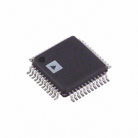
AD9218BSTZ-105 Analog Devices Inc, AD9218BSTZ-105 Datasheet - Page 21

AD9218BSTZ-105
Manufacturer Part Number
AD9218BSTZ-105
Description
IC ADC 10BIT DUAL 105MSPS 48LQFP
Manufacturer
Analog Devices Inc
Datasheet
1.AD9218BSTZ-40.pdf
(28 pages)
Specifications of AD9218BSTZ-105
Data Interface
Parallel
Number Of Bits
10
Sampling Rate (per Second)
105M
Number Of Converters
2
Power Dissipation (max)
565mW
Voltage Supply Source
Analog and Digital
Operating Temperature
-40°C ~ 85°C
Mounting Type
Surface Mount
Package / Case
48-LQFP
Resolution (bits)
10bit
Sampling Rate
105MSPS
Input Channel Type
Differential
Supply Voltage Range - Analog
2.7V To 3.6V
Lead Free Status / RoHS Status
Lead free / RoHS Compliant
Available stocks
Company
Part Number
Manufacturer
Quantity
Price
Company:
Part Number:
AD9218BSTZ-105
Manufacturer:
ADI
Quantity:
455
Company:
Part Number:
AD9218BSTZ-105
Manufacturer:
Analog Devices Inc
Quantity:
10 000
Part Number:
AD9218BSTZ-105
Manufacturer:
ADI/亚德诺
Quantity:
20 000
EVALUATION BOARD
The AD9218/AD9288 customer evaluation board offers an easy
way to test the AD9218 or the AD9288. The compatible pinout
of the two parts facilitates the use of one PCB for testing either
part. The PCB requires power supplies, a clock source, and a
filtered analog source for most ADC testing required.
POWER CONNECTOR
Power is supplied to the board via a detachable 12-lead power
strip. The minimum 3 V supplies required to run the board are
V
path, ±5 V supplies are required.
ANALOG INPUTS
Each channel has an independent analog path that uses a
wideband transformer to drive the ADC differentially from a
single-ended sine source at the input SMAs. The transformer
paths can be bypassed to allow the use of a dc-coupled path
using two AD8138 op amps with a simple board modification.
The analog input should be band-pass filtered to remove any
harmonics in the input signal and to minimize aliasing.
VOLTAGE REFERENCE
The AD9218 has an internal 1.25 V voltage reference; an
external reference for each channel can be employed instead
by connecting two external voltage references at the power
connector and setting jumpers at E18 and E19. The evaluation
board is shipped configured for internal reference mode.
CLOCKING
Each channel can be clocked by a common clock input at SMA
inputs ENCODE A and ENCODE B. The channels can also be
clocked independently by a simple board modification. The
clock input should be a low jitter sine source for maximum
performance.
D
, V
DL
, and V
DD
. To allow the use of the optional amplifier
Rev. C | Page 21 of 28
DATA OUTPUTS
The data outputs are latched on board by two 10-bit latches
and drive an 8-lead connector, which is compatible with the dual-
channel FIFO board that is available from Analog Devices, Inc.
This board, together with ADC analyzer software, can greatly
simplify ADC testing.
DATA FORMAT/GAIN
The DFS/GAIN pin can be biased for desired operation at the
DFS jumper located at the S1, S2 jumpers.
TIMING
Timing on each channel can be controlled, if needed, on the
PCB. Clock signals at the latches or the data ready signals that
go to the output 80-lead connector can be inverted if required.
Jumpers also allow for biasing of Pin S1 and Pin S2 for power-
down and timing alignment control.
TROUBLESHOOTING
If the board does not seem to be working correctly, try the
following:
• Verify power at the IC pins.
• Check that all jumpers are in the correct position for the
• Verify that V
• Try running encode clock and analog inputs at low speeds
The AD9218 evaluation board is provided as a design example
for customers of Analog Devices. Analog Devices makes no
warranties, express, statutory, or implied, regarding
merchantability or fitness for a particular purpose.
desired mode of operation.
(20 MSPS/1 MHz) and monitor the LCX821 outputs, DAC
outputs, and ADC outputs for toggling.
REF
is at 1.23 V.
AD9218


