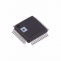
AD9218BSTZ-105 Analog Devices Inc, AD9218BSTZ-105 Datasheet - Page 9

AD9218BSTZ-105
Manufacturer Part Number
AD9218BSTZ-105
Description
IC ADC 10BIT DUAL 105MSPS 48LQFP
Manufacturer
Analog Devices Inc
Datasheet
1.AD9218BSTZ-40.pdf
(28 pages)
Specifications of AD9218BSTZ-105
Data Interface
Parallel
Number Of Bits
10
Sampling Rate (per Second)
105M
Number Of Converters
2
Power Dissipation (max)
565mW
Voltage Supply Source
Analog and Digital
Operating Temperature
-40°C ~ 85°C
Mounting Type
Surface Mount
Package / Case
48-LQFP
Resolution (bits)
10bit
Sampling Rate
105MSPS
Input Channel Type
Differential
Supply Voltage Range - Analog
2.7V To 3.6V
Lead Free Status / RoHS Status
Lead free / RoHS Compliant
Available stocks
Company
Part Number
Manufacturer
Quantity
Price
Company:
Part Number:
AD9218BSTZ-105
Manufacturer:
ADI
Quantity:
455
Company:
Part Number:
AD9218BSTZ-105
Manufacturer:
Analog Devices Inc
Quantity:
10 000
Part Number:
AD9218BSTZ-105
Manufacturer:
ADI/亚德诺
Quantity:
20 000
PIN CONFIGURATION AND FUNCTION DESCRIPTIONS
Table 7. Pin Function Descriptions
Pin Number
1, 12, 16, 27, 29,
32, 34, 45
2
3
4
5
6
7
8
9
10
11
13, 30, 31, 48
14
15, 28, 33, 46
17 to 26
35 to 44
47
Mnemonic
GND
A
DFS/GAIN
REF
REF
REF
S1
S2
A
V
ENC
V
D9 to D0
D0
ENC
A
A
D
DD
IN
IN
IN
IN
A
B
B
A
A
B
IN
OUT
IN
B
A
to D9
A
B
B
A
Description
Ground.
Analog Input for Channel A.
Analog Input for Channel A (Complementary).
Data Format Select and Analog Input Gain Mode. Low = offset binary output available, 1 V p-p supported;
high = twos complement output available, 1 V p-p supported; floating = offset binary output available,
2 V p-p supported; set to V
Reference Voltage Input for Channel A.
Internal Reference Voltage.
Reference Voltage Input for Channel B.
User Select No. 1. See Table 6.
User Select No. 2. See Table 6.
Analog Input for Channel B (Complementary).
Analog Input for Channel B.
Analog Supply (3 V).
Clock Input for Channel B.
Digital Supply (2.5 V to 3.6 V).
Digital Output for Channel B (D9 = MSB).
Digital Output for Channel A (D9
Clock Input for Channel A.
DFS/GAIN
REF
REF
REF
A
A
GND
A
A
GND
OUT
IN
IN
IN
IN
IN
IN
S1
S2
A
A
A
B
B
B
10
11
12
1
2
3
4
5
6
7
8
9
Figure 5. Pin Configuration
REF
Rev. C | Page 9 of 28
= twos complement output available, 2 V p-p supported.
(Not to Scale)
AD9218
TOP VIEW
B
A
= MSB).
36
35
34
33
32
31
30
29
28
27
26
25
D1
D0
GND
V
GND
V
V
GND
V
GND
D0
D1
DD
D
D
DD
A
A
B
B
AD9218


