ADC10158CIWMX/NOPB National Semiconductor, ADC10158CIWMX/NOPB Datasheet - Page 17
ADC10158CIWMX/NOPB
Manufacturer Part Number
ADC10158CIWMX/NOPB
Description
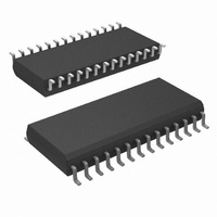
IC ADC 10BIT 28-SOIC
Manufacturer
National Semiconductor
Datasheet
1.ADC10158CIWMNOPB.pdf
(23 pages)
Specifications of ADC10158CIWMX/NOPB
Number Of Bits
10
Sampling Rate (per Second)
166k
Number Of Converters
1
Power Dissipation (max)
33mW
Voltage Supply Source
Analog and Digital, Dual ±
Operating Temperature
-40°C ~ 85°C
Mounting Type
Surface Mount
Package / Case
28-SOIC (0.300", 7.50mm Width)
Lead Free Status / RoHS Status
Lead free / RoHS Compliant
Other names
*ADC10158CIWMX
*ADC10158CIWMX/NOPB
ADC10158CIWMX
*ADC10158CIWMX/NOPB
ADC10158CIWMX
Available stocks
Company
Part Number
Manufacturer
Quantity
Price
Company:

Part Number:
ADC10158CIWMX/NOPB
Manufacturer:
NS
Quantity:
7 872
Company:
Part Number:
ADC10158CIWMX/NOPB
Manufacturer:
NS
Quantity:
6 000


1.0 Functional Description
Digital Interface Hints:
1) When initiating a write, CS and WR must be simulta-
2) When reading data, understand that data will not be valid
1.2 ARCHITECTURE
Before a conversion is started, during the analog input sam-
pling period, the sampled data comparator is zeroed. As the
comparator is being zeroed the channel assigned to be the
positive input is connected to the A/D’s input capacitor. (See
the Digital Interface section for a description of the assign-
ment procedure.) This charges the input 32C capacitor of the
DAC to the positive analog input voltage. The switches
shown in the DAC portion of the detailed block diagram are
set for this zeroing/acquisition period. The voltage at the
input and output of the comparator are at equilibrium at this
point in time. When the conversion is started the comparator
feedback switches are opened and the 32C input capacitor
is then switched to the assigned negative input voltage.
When the comparator feedback switch opens a fixed amount
of charge is trapped on the common plates of the capacitors.
The voltage at the input of the comparator moves away from
equilibrium when the 32C capacitor is switched to the as-
signed negative input voltage, causing the output of the
comparator to go high (“1”) or low (“0”). The SAR next goes
through an algorithm, controlled by the output state of the
comparator, that redistributes the charge on the capacitor
array by switching the voltage on one side of the capacitors
in the array. The objective of the SAR algorithm is to return
the voltage at the input of the comparator as close as pos-
sible to equilibrium.
The switch position information at the completion of the
successive approximation routine is a direct representation
•
•
•
Reads and writes can be completely asynchronous to
CLK.
In addition to the timing indicated in Diagrams 1–3, CS
can be tied low permanently or taken low for entire
conversions, eliminating all the CS guardbands (t
t
If CS is used as shown in Diagrams 1–-3, the CS guard-
bands (t
WR signals can safely be ignored as long as the follow-
ing two conditions are met:
neously low for at least t
“start” conversion” bit will be set on the rising edge of WR
or CS, whichever is first.
until t
data will enter TRI-STATE t
or RD goes high (see Diagrams 2 and 3).
CW
, t
WC
ACC
CR
).
ns after both CS and RD go low. The output
, t
RC
, t
CW
, t
WC
W(WR)
) between CS and the RD and
1H
ns or t
ns (see Diagram 1). The
0H
ns after either CS
(Continued)
CR
, t
RC
,
17
of the digital output. This information is then manipulated by
the Digital Output decoder to the programmed format. The
reformatted data is then available to be strobed onto the data
bus (DB0–DB7) via the digital output buffers by taking CS
and RD low.
2.0 Applications Information
2.1 MULTIPLEXER CONFIGURATION
The design of these converters utilizes a sampled-data com-
parator structure which allows a differential analog input to
be converted by the successive approximation routine.
The actual voltage converted is always the difference be-
tween an assigned “+” input terminal and a “−” input terminal.
The polarity of each input terminal or pair of input terminals
being converted indicates which line the converter expects
to be the most positive. If the assigned “+” input is less than
the “−” input the converter responds with an all zeros output
code when configured for unsigned operation. When config-
ured for signed operation the A/D responds with the appro-
priate output digital code.
A unique input multiplexing scheme has been utilized to
provide multiple analog channels. The input channels can be
software
single-ended, or pseudo-differential. Figure 4 shows the
three modes using the 4-channel MUX of the ADC10154.
The eight inputs of the ADC10158 can also be configured in
any of the three modes. The single-ended mode has
CH0–CH3 assigned as the positive input with the negative
input being the V
the ADC10154 channel inputs are grouped in pairs, CH0
with CH1 and CH2 with CH3. The polarity assignment of
each channel in the pair is interchangeable. Finally, in the
pseudo-differential mode CH0–CH2 are positive inputs re-
ferred to CH3 which is now a pseudo-ground. This
pseudo-ground input can be set to any potential within the
input common-mode range of the converter. The analog
signal conditioning required in transducer-based data acqui-
sition systems is significantly simplified with this type of input
flexibility.
ground-referred inputs and true differential inputs as well as
signals referred to a specific voltage.
The analog input voltages for each channel can range from
50 mV below V
−5V for bipolar operation) to 50 mV above V
(typically 5V) without degrading conversion accuracy. If the
voltage on an unselected channel exceeds these limits it
may corrupt the reading of the selected channel.
configured
One
−
REF
(typically ground for unipolar operation or
converter
−
of the device. In the differential mode,
into
package
three
modes:
can
+
now
= DV
www.national.com
differential,
+
handle
= AV
+
Related parts for ADC10158CIWMX/NOPB
Image
Part Number
Description
Manufacturer
Datasheet
Request
R

Part Number:
Description:
National Semiconductor [8-Bit D/A Converter]
Manufacturer:
National Semiconductor
Datasheet:
Part Number:
Description:
National Semiconductor [Media Coprocessor]
Manufacturer:
National Semiconductor
Datasheet:
Part Number:
Description:
Digitally Controlled Tone and Volume Circuit with Stereo Audio Power Amplifier, Microphone Preamp Stage and National 3D Sound
Manufacturer:
National Semiconductor
Datasheet:
Part Number:
Description:
Digitally Controlled Tone and Volume Circuit with Stereo Audio Power Amplifier, Microphone Preamp Stage and National 3D Sound
Manufacturer:
National Semiconductor
Datasheet:
Part Number:
Description:
AC97 Rev 2 Codec with Sample Rate Conversion and National 3D Sound
Manufacturer:
National Semiconductor
Part Number:
Description:
Manufacturer:
National Semiconductor
Datasheet:
Part Number:
Description:
Manufacturer:
National Semiconductor
Datasheet:
Part Number:
Description:
General Purpose, Low Voltage, Low Power, Rail-to-Rail Output Operational Amplifiers
Manufacturer:
National Semiconductor
Datasheet:
Part Number:
Description:
8-bit 20 MSPS flash A/D converter.
Manufacturer:
National Semiconductor
Datasheet:
Part Number:
Description:
Low Noise Quad Operational Amplifier
Manufacturer:
National Semiconductor
Datasheet:
Part Number:
Description:
Quad Differential Line Receivers
Manufacturer:
National Semiconductor
Datasheet:
Part Number:
Description:
Quad High Speed Trapezoidal? Bus Transceiver
Manufacturer:
National Semiconductor
Datasheet:
Part Number:
Description:
Dual Line Receiver
Manufacturer:
National Semiconductor
Datasheet:
Part Number:
Description:
TTL to 10k ECL Level Translator with Latch
Manufacturer:
National Semiconductor
Datasheet: