ADC10154CIWMX/NOPB National Semiconductor, ADC10154CIWMX/NOPB Datasheet - Page 7
ADC10154CIWMX/NOPB
Manufacturer Part Number
ADC10154CIWMX/NOPB
Description
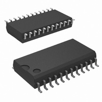
IC ADC 10BIT 24-SOIC
Manufacturer
National Semiconductor
Datasheet
1.ADC10158CIWMNOPB.pdf
(23 pages)
Specifications of ADC10154CIWMX/NOPB
Number Of Bits
10
Sampling Rate (per Second)
166k
Number Of Converters
1
Power Dissipation (max)
33mW
Voltage Supply Source
Analog and Digital, Dual ±
Operating Temperature
-65°C ~ 150°C
Mounting Type
Surface Mount
Package / Case
24-SOIC (0.300", 7.50mm Width)
Lead Free Status / RoHS Status
Lead free / RoHS Compliant
Other names
*ADC10154CIWMX
*ADC10154CIWMX/NOPB
ADC10154CIWMX
*ADC10154CIWMX/NOPB
ADC10154CIWMX
Available stocks
Company
Part Number
Manufacturer
Quantity
Price
Company:

Part Number:
ADC10154CIWMX/NOPB
Manufacturer:
NS
Quantity:
7 882


Electrical Characteristics
Note 1: Absolute Maximum Ratings indicate limits beyond which damage to the device may occur.
Note 2: Operating Ratings indicate conditions for which the device is functional, but do not guarantee specific performance limits. For guaranteed specifications and
test conditions, see the Electrical Characteristics. The guaranteed specifications apply only for the test conditions listed. Some performance characteristics may
degrade when the device is not operated under the listed test conditions.
Note 3: All voltages are measured with respect to GND, unless otherwise specified.
Note 4: When the input voltage (V
20 mA maximum package input current rating limits the number of pins that can safely exceed the power supplies with an input current of 5 mA to four.
Note 5: The maximum power dissipation must be derated at elevated temperatures and is dictated by T
allowable power dissipation at any temperature is P
T
CIJ and CMJ suffixes 49˚C/W, ADC10154 with BIWM and CIWM suffixes 72˚C/W, ADC10158 with BIN and CIN suffixes 59˚C/W, ADC10158 with BIJ, CIJ, and CMJ
suffixes 46˚C/W, ADC10158 with BIWM and CIWM suffixes 68˚C/W.
Note 6: Human body model, 100 pF capacitor discharged through a 1.5 k
Note 7: See AN-450 “Surface Mounting Methods and Their Effect on Product Reliability” or the section titled “Surface Mount” found in any post-1986 National
Semiconductor Linear Data Book for other methods of soldering surface mount devices.
Note 8: Two on-chip diodes are tied to each analog input as shown below. They will forward-conduct for analog input voltages one diode drop below V
especially at elevated temperatures, which will cause errors for analog inputs near full-scale. The specification allows 50 mV forward bias of either diode; this means
that as long as the analog V
channel will corrupt the reading of a selected channel. This means that if AV
Note 9: A diode exists between AV
To guarantee accuracy, it is required that the AV
Note 10: Typicals are at T
Note 11: Tested limits are guaranteed to National’s AOQL (Average Outgoing Quality Level).
Note 12: One LSB is referenced to 10 bits of resolution.
Note 13: Total unadjusted error includes offset, full-scale, linearity, multiplexer, and hold step errors.
Note 14: For DC Common Mode Error the only specification that is measured is offset error.
Note 15: Channel leakage current is measured after the channel selection.
Note 16: All the timing specifications are tested at the TTL logic levels, V
one diode drop greater than V
Jmax
±
4.55 V
= 150˚C. The typical thermal resistance (
DC
.
J
IN
= T
+
does not exceed the supply voltage by more than 50 mV, the output code will be correct. Exceeding this range on an unselected
A
supply. Be careful during testing at low V
= 25˚C and represent most likely parametric norm.
IN
+
) at any pin exceeds the power supplies (V
and DV
+
as shown below.
JA
+
and DV
) of these parts when board mounted follow: ADC10154 with BIN and CIN suffixes 65˚C/W, ADC10154 with BIJ,
D
= (T
(Continued)
Jmax
+
be connected together to a power supply with separate bypass filter at each V
− T
A
)/
JA
or the number given in the Absolute Maximum Ratings, whichever is lower. For this device,
IL
+
+
= 0.8V for a falling edge and V
levels (4.5V), as high level analog inputs (5V) can cause an input diode to conduct,
resistor.
and DV
IN
7
<
V
+
−
are minimum (4.5 V
or V
IN
DS011225-5
>
AV
+
or DV
DS011225-4
Jmax
+
DC
), the current at that pin should be limited to 5 mA. The
IH
,
) and V
= 2.0V for a rising.
JA
and the ambient temperature, T
−
is a maximum (−4.5 V
+
DC
pin.
) full scale must be
A
. The maximum
www.national.com
−
supply or
Related parts for ADC10154CIWMX/NOPB
Image
Part Number
Description
Manufacturer
Datasheet
Request
R

Part Number:
Description:
National Semiconductor [8-Bit D/A Converter]
Manufacturer:
National Semiconductor
Datasheet:
Part Number:
Description:
National Semiconductor [Media Coprocessor]
Manufacturer:
National Semiconductor
Datasheet:
Part Number:
Description:
Digitally Controlled Tone and Volume Circuit with Stereo Audio Power Amplifier, Microphone Preamp Stage and National 3D Sound
Manufacturer:
National Semiconductor
Datasheet:
Part Number:
Description:
Digitally Controlled Tone and Volume Circuit with Stereo Audio Power Amplifier, Microphone Preamp Stage and National 3D Sound
Manufacturer:
National Semiconductor
Datasheet:
Part Number:
Description:
AC97 Rev 2 Codec with Sample Rate Conversion and National 3D Sound
Manufacturer:
National Semiconductor
Part Number:
Description:
Manufacturer:
National Semiconductor
Datasheet:
Part Number:
Description:
Manufacturer:
National Semiconductor
Datasheet:
Part Number:
Description:
General Purpose, Low Voltage, Low Power, Rail-to-Rail Output Operational Amplifiers
Manufacturer:
National Semiconductor
Datasheet:
Part Number:
Description:
8-bit 20 MSPS flash A/D converter.
Manufacturer:
National Semiconductor
Datasheet:
Part Number:
Description:
Low Noise Quad Operational Amplifier
Manufacturer:
National Semiconductor
Datasheet:
Part Number:
Description:
Quad Differential Line Receivers
Manufacturer:
National Semiconductor
Datasheet:
Part Number:
Description:
Quad High Speed Trapezoidal? Bus Transceiver
Manufacturer:
National Semiconductor
Datasheet:
Part Number:
Description:
Dual Line Receiver
Manufacturer:
National Semiconductor
Datasheet:
Part Number:
Description:
TTL to 10k ECL Level Translator with Latch
Manufacturer:
National Semiconductor
Datasheet: