ADC0848BCJ National Semiconductor, ADC0848BCJ Datasheet
ADC0848BCJ
Specifications of ADC0848BCJ
Available stocks


Related parts for ADC0848BCJ

ADC0848BCJ Summary of contents
Page 1
... A/ config- ured as memory locations or I/O devices to the microproces- sor with no interface logic necessary. Block Diagram * ADC0848 shown in DIP Package CH5-CH8 not included on the ADC0844 © 2008 National Semiconductor Corporation Features ■ Easy interface to all microprocessors ■ ...
Page 2
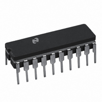
Connection Diagrams Molded Chip Carrier Package Top View See Ordering Information Dual-In-Line Package Top View Ordering Information Temperature Total Unadjusted Error Range ±½ 0°C to +70°C ADC0848BCN ADC0844BCJ* −40°C to +85°C ADC0848BCV ADC0848BCVX ADC0848CCVX * Product/package combination obsolete; shown for ...
Page 3
... Absolute Maximum Ratings If Military/Aerospace specified devices are required, please contact the National Semiconductor Sales Office/ Distributors for availability and specifications. Supply Voltage ( Voltage Logic Control Inputs At Other Inputs and Outputs Input Current at Any Pin (Note 3) Package Input Current (Note 3) Storage Temperature Package Dissipation at T =25° ...
Page 4
Parameter V , Logical “0” Output Voltage (Max) OUT( TRI-STATE Output Current (Max) OUT I , Output Source Current (Min) SOURCE I , Output Sink Current (Min) SINK I , Supply Current (Max Electrical Characteristics The ...
Page 5
Typical Performance Characteristics Logic Input Threshold Voltage vs. Supply Voltage Power Supply Current vs. Temperature Conversion Time vs. V 501631 501633 SUPPLY 501635 5 Output Current vs. Temperature 501632 Linearity Error vs. V REF 501634 Conversion Time vs. Temperature 501636 ...
Page 6
Unadjusted Offset Error vs. V Voltage REF TRI-STATE Test Circuits and Waveforms www.national.com 501637 501604 501606 501605 ...
Page 7
Leakage Current Test Circuit Timing Diagrams Programming New Channel Configuration and Starting a Conversion Note 13: Read strobe must occur at least 600 ns after the assertion of interrupt to guarantee reset of INTR . Note 14: MA stands for ...
Page 8
www.national.com 8 501610 ...
Page 9
9 www.national.com ...
Page 10
Functional Description The ADC0844 and ADC0848 contain a 4-channel and 8- channel analog input multiplexer (MUX) respectively. Each MUX can be configured into one of three modes of operation differential, pseudo-differential, and single ended. These modes are discussed in the ...
Page 11
REFERENCE CONSIDERATIONS The voltage applied to the reference input of these converters defines the voltage span of the analog input (the difference between V and V ) over which the 256 possible IN(MAX) IN(MIN) output codes apply. The devices ...
Page 12
THE ANALOG INPUTS 3.1 Analog Differential Voltage Inputs and Common- Mode Rejection The differential input of these converters actually reduces the effects of common-mode input noise, a signal common to both selected “+” and “−” inputs for a conversion ...
Page 13
V − input and applying a small magnitude pos- itive voltage to the V + input. Zero error is the difference between actual DC input voltage which is necessary to just cause an output digital code transition from ...
Page 14
For an example see the Zero-Shift and Span Adjust circuit below. www.national.com ≤ ≤ Zero-Shift and Span Adjust ( Differential Voltage Input 9-Bit A/D 14 5V) 501618 501619 ...
Page 15
Diodes are 1N914 DO = all (+)>V (− all (+)<V (− ≤ ≤ Span Adjust (0V V 3V) IN Protecting the Input High Accuracy Comparators 501622 15 501620 ...
Page 16
V (−)=0. ≤ ≤ XDR CC www.national.com Operating with Automotive Ratiometric Transducers 16 501623 ...
Page 17
Note: DUT pin numbers in parentheses are for ADC0844, others are for ADC0848. Start a Conversion without Updating the Channel Configuration CS •WR will update the channel configuration and start a conversion. CS •RD will read the conversion data and ...
Page 18
SAMPLE PROGRAM FOR ADC0844—INS8039 INTERFACE CONVERTING TWO RATIOMETRIC, DIFFERENTIAL SIGNALS 0000 04 10 0010 B9 FF BEGIN: 0012 B8 20 0014 89 FF 0016 23 00 0018 14 50 001A 23 02 001C 18 001D 14 50 0050 99 FE ...
Page 19
SAMPLE PROGRAM FOR ADC0848—NSC800 INTERFACE 0008 NCONV 000F DEL 001F CS 3C00 ADDTA ′ MUXDTA: 0000 ′ 0004 ′ START: 0008 ′ 000A ′ ′ 000C 21 0000 ...
Page 20
Physical Dimensions Ceramic Dual-In-Line Package (J) (product obsolete in this package) www.national.com inches (millimeters) unless otherwise noted NS Package Number J20A Molded Dual-In-Line Package (N) NS Package Number N20A 20 ...
Page 21
Molded Dual-In-Line Package (N) NS Package Number N24D 21 www.national.com ...
Page 22
Molded Chip Carrier Package (V) NS Package Number V28A 22 ...
Page 23
Notes 23 www.national.com ...
Page 24
... For more National Semiconductor product information and proven design tools, visit the following Web sites at: Products Amplifiers www.national.com/amplifiers Audio www.national.com/audio Clock and Timing www.national.com/timing Data Converters www.national.com/adc Interface www.national.com/interface LVDS www.national.com/lvds Power Management www.national.com/power Switching Regulators www.national.com/switchers LDOs www.national.com/ldo LED Lighting www ...