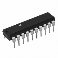
ADC08061CIN National Semiconductor, ADC08061CIN Datasheet

ADC08061CIN
Specifications of ADC08061CIN
Available stocks
Related parts for ADC08061CIN
ADC08061CIN Summary of contents
Page 1
... S H The digital interface has been designed to ease connection to microprocessors and allows the parts memo- ry mapped Block Diagram ADC08061 ADC08062 TRI-STATE is a registered trademark of National Semiconductor Corporation C 1996 National Semiconductor Corporation TL H 11086 Key Specifications Resolution Y Conversion Time ...
Page 2
... Absolute Maximum Ratings If Military Aerospace specified devices are required please contact the National Semiconductor Sales Office Distributors for availability and specifications Supply Voltage ( Logic Control Inputs b Voltage at Other Inputs and Outputs b Input Current at Any Pin (Note 3) Package Input Current (Note 3) Power Dissipation (Note 4) ...
Page 3
AC Electrical Characteristics The following specifications apply for V a Boldface limits apply for Symbol Parameter t Write Time WR t Read Time (Time from Falling Edge Mode Pin ...
Page 4
DC Electrical Characteristics Boldface limits apply for Symbol Parameter V Logic ‘‘1’’ Input Voltage IH V Logic ‘‘0’’ Input Voltage IL I Logic ‘‘1’’ Input Current IH I Logic ‘‘0’’ Input Current IL V Logic ...
Page 5
Electrical Characteristics (Continued) Note 1 Absolute Maximum Ratings indicate limits beyond which damage to the device may occur DC and AC electrical specifications do not apply when operating the device beyond its specified operating ratings Operating Ratings indicate conditions for ...
Page 6
TRI-STATE Test Circuits and Waveforms Timing Diagrams http www national com TL H 11086– 11086–3 FIGURE 1 RD Mode (Mode Pin is Low 11086 ...
Page 7
Timing Diagrams (Continued) FIGURE 2a WR-RD Mode (Mode Pin is High and t FIGURE 2b WR-RD Mode (Mode Pin is High and INTL INTL 11086 – ...
Page 8
Timing Diagrams (Continued) FIGURE 3 WR-RD Mode (Mode Pin is High) Reduced Interface System Connection (CS FIGURE 4 RD Mode (Pipeline Operation) (Mode Pin is Low and t http www national com e must be between 200 ns and 400 ...
Page 9
... Temperature CRD Supply Current vs Temperature Connection Diagrams Dual-In-Line and Wide-Body Small-Outline Packages J20A N20A or M20B Ordering Information Industrial ( ADC08061BIN ADC08061CIN ADC08062BIN ADC08062CIN ADC08061BIWM ADC08061CIWM ADC08062BIWM ADC08062CIWM ADC08061CMJ 883 5962 Linearity Error vs Reference Voltage Logic Threshold vs Temperature TL H 11086 – 14 Dual-In-Line and Wide-Body ...
Page 10
Pin Description V V These are analog inputs The input range is IN IN1 –8 GND– INPUT s ADC08061 has a single input (V ADC08062 has a two-channel multiplexer (V ) IN1 – 2 DB0 –DB7 ...
Page 11
Application Information 1 0 FUNCTIONAL DESCRIPTION The ADC08061 and ADC08062 perform an 8-bit analog-to- digital conversion using a multi-step flash technique The first flash generates the five most significant bits (MSBs) and the second flash generates the three least significant ...
Page 12
Application Information A conversion begins with the Voltage Estimator comparing the analog input signal against the six tap voltages on the estimator DAC The estimator decoder then selects one of the groups of tap points along the MSB Ladder These ...
Page 13
Application Information (Continued) shows the input code needed to select a given channel The multiplexer address is latched when received but the multi- plexer channel is updated after the completion of the cur- rent conversion TABLE I Multiplexer Addressing ADC08062 ...
Page 14
Application Information External Reference 2 5V Full-Scale (Standard Application 11086– 20 Note Bypass capacitors consist ceramic in parallel with bead tantalum Note the multiple bypass capacitors on the reference and ...
Page 15
Physical Dimensions inches (millimeters) Order Number ADC08061CMJ or ADC08061CMJ 883 5962 Wide-Body Small-Outline Package (M) Order Number ADC08061BIWM ADC08061CIWM ADC08062BIWM or ADC08062CIWM Ceramic Dual-In-Line Package (J) NS Package Number J20A NS Package Number M20B 15 http www national com ...
Page 16
... Physical Dimensions inches (millimeters) (Continued) Order Number ADC08061BIN ADC08061CIN ADC08062BIN or ADC08062CIN LIFE SUPPORT POLICY NATIONAL’S PRODUCTS ARE NOT AUTHORIZED FOR USE AS CRITICAL COMPONENTS IN LIFE SUPPORT DEVICES OR SYSTEMS WITHOUT THE EXPRESS WRITTEN APPROVAL OF THE PRESIDENT OF NATIONAL SEMICONDUCTOR CORPORATION As used herein 1 Life support devices or systems are devices or ...


