LM12458CIV/NOPB National Semiconductor, LM12458CIV/NOPB Datasheet - Page 28
LM12458CIV/NOPB
Manufacturer Part Number
LM12458CIV/NOPB
Description
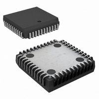
IC ACQUISITION SYS 12BIT 44-PLCC
Manufacturer
National Semiconductor
Type
Data Acquisition System (DAS)r
Datasheet
1.LM12458CIVNOPB.pdf
(36 pages)
Specifications of LM12458CIV/NOPB
Resolution (bits)
12 b
Sampling Rate (per Second)
140k
Data Interface
Parallel
Voltage Supply Source
Analog and Digital
Voltage - Supply
3 V ~ 5.5 V
Operating Temperature
-40°C ~ 85°C
Mounting Type
Surface Mount
Package / Case
44-PLCC
Lead Free Status / RoHS Status
Lead free / RoHS Compliant
Other names
*LM12458CIV
*LM12458CIV/NOPB
LM12458CIV
*LM12458CIV/NOPB
LM12458CIV
Available stocks
Company
Part Number
Manufacturer
Quantity
Price
Company:

Part Number:
LM12458CIV/NOPB
Manufacturer:
Zilog
Quantity:
101
Company:
Part Number:
LM12458CIV/NOPB
Manufacturer:
Texas Instruments
Quantity:
10 000


www.national.com
2.0 Internal User-Programmable
Registers
mand (“1”) disconnects the external clock from the internal
circuitry, decreases the LM12(H)454/8’s internal analog cir-
cuitry power supply current, and preserves all internal RAM
contents. After writing a “0” to the Standby bit, the
LM12(H)454/8 returns to an operating state identical to that
caused by exercising the RESET bit. A Standby completion
interrupt is issued after a power-up completion delay that
allows the analog circuitry to settle. The Sequencer should
be restarted only after the Standby completion is issued. The
Instruction RAM can still be accessed through read and write
operations while the LM12(H)454/8 are in Standby Mode.
Bit 5 is the Channel Address Mask. If Bit 5 is set to a “1”, Bits
13–15 in the conversion FIFO will be equal to the sign bit (Bit
12) of the conversion data. Resetting Bit 5 to a “0” causes
conversion data Bits 13 through 15 to hold the instruction
pointer value of the instruction to which the conversion data
belongs.
Bit 6 is used to select a “short” auto-zero correction for every
conversion. The Sequencer automatically inserts an auto-
zero before every conversion or “watchdog” comparison if
Bit 6 is set to “1”. No automatic correction will be performed
if Bit 6 is reset to “0”.
The LM12(H)454/8’s offset voltage, after calibration, has a
typical drift of 0.1 LSB over a temperature range of −40˚C to
+85˚C. This small drift is less than the variability of the
change in offset that can occur when using the auto-zero
correction with each conversion. This variability is the result
of using only one sample of the offset voltage to create a
correction value. This variability decreases when using the
full calibration mode because eight samples of the offset
voltage are taken, averaged, and used to create a correction
value.
Bit 7 is used to program the SYNC pin (29) to operate as
either an input or an output. The SYNC pin becomes an
output when Bit 7 is a “1” and an input when Bit 7 is a “0”.
With SYNC programmed as an input, the rising edge of any
logic signal applied to pin 29 will start a conversion or
“watchdog” comparison. Programmed as an output, the logic
level at pin 29 will go high at the start of a conversion or
“watchdog” comparison and remain high until either have
finished. See Instruction RAM “00”, Bit 8.
Bits 8 and 9 form the RAM Pointer that is used to select
each of a 48-bit instruction’s three 16-bit sections during
read or write actions. A “00” selects Instruction RAM section
one, “01” selects section two, and “10” selects section three.
Bit 10 activates the Test mode that is used only during
production testing. Leave this bit reset to “0”.
Bit 11 is the Diagnostic bit and is available only in the
LM12(H)458. It can be activated by setting it to a “1” (the Test
bit must be reset to a “0”). The Diagnostic mode, along with
a correctly chosen instruction, allows verification that the
LM12(H)458’s ADC is performing correctly. When activated,
the inverting and non-inverting inputs are connected as
shown in Table 1. As an example, an instruction with “001”
for both V
typically results in a full-scale output.
2.3 INTERRUPTS
The LM12454 and LM12(H)458 have eight possible inter-
rupts, all with the same priority. Any of these interrupts will
cause a hardware interrupt to appear on the INT pin (31) if
IN+
and V
(Continued)
IN−
while using the Diagnostic mode
28
they are not masked (by the Interrupt Enable register). The
Interrupt Status register is then read to determine which of
the eight interrupts has been issued.
The Interrupt Status register, 1010 (A4–A1, BW = 0) or
1010x (A4–A0, BW = 1) must be cleared by reading it after
writing to the Interrupt Enable register. This removes any
spurious interrupts on the INT pin generated during an Inter-
rupt Enable register access.
Interrupt 0 is generated whenever the analog input voltage
on a selected multiplexer channel crosses a limit while the
LM12(H)454/8 are operating in the “watchdog” comparison
mode. Two sequential comparisons are made when the
LM12(H)454/8 are executing a “watchdog” instruction. De-
pending on the logic state of Bit 9 in the Instruction RAM’s
second and third sections, an interrupt will be generated
either when the input signal’s magnitude is greater than or
less than the programmable limits. (See the Instruction
RAM, Bit 9 description.) The Limit Status register will indicate
which preprogrammed limit, #1 or #2 and which instruction
was executing when the limit was crossed.
Interrupt 1 is generated when the Sequencer reaches the
instruction counter value specified in the Interrupt Enable
register’s bits 8–10. This flag appears before the instruc-
tion’s execution.
Interrupt 2 is activated when the Conversion FIFO holds a
number of conversions equal to the programmable value
stored in the Interrupt Enable register’s Bits 11–15. This
value ranges from 0001 to 1111, representing 1 to 31 con-
versions stored in the FIFO. A user-programmed value of
0000 has no meaning. See Section 3.0 for more FIFO infor-
mation.
NOTE: The LM12(H)454 is no longer available.
Information shown for reference only.
Channel Selection
Selection
Channel
Data
000
001
010
011
100
101
110
111
Channel Configuration Showing Normal
TABLE 1. LM12(H)458 Input Multiplexer
Data
1XX
000
001
010
011
TABLE 2. LM12454 Input Multiplexer
Mode and Diagnostic Mode
V
Normal Mode
Channel Configuration
IN0
IN1
IN2
IN3
IN4
IN5
IN6
IN7
IN+
GND
V
IN1
IN2
IN3
IN4
IN5
IN6
IN7
IN−
MUX+
OPEN
IN0
IN1
IN2
IN3
V
Diagnostic Mode
V
REFOUT
V
IN2
IN3
IN4
IN5
IN6
IN7
REF+
IN+
MUX−
OPEN
GND
IN1
IN2
IN3
V
GND
V
IN2
IN3
IN4
IN5
IN6
IN7
REF−
IN−
Related parts for LM12458CIV/NOPB
Image
Part Number
Description
Manufacturer
Datasheet
Request
R

Part Number:
Description:
National Semiconductor [8-Bit D/A Converter]
Manufacturer:
National Semiconductor
Datasheet:
Part Number:
Description:
National Semiconductor [Media Coprocessor]
Manufacturer:
National Semiconductor
Datasheet:
Part Number:
Description:
Digitally Controlled Tone and Volume Circuit with Stereo Audio Power Amplifier, Microphone Preamp Stage and National 3D Sound
Manufacturer:
National Semiconductor
Datasheet:
Part Number:
Description:
Digitally Controlled Tone and Volume Circuit with Stereo Audio Power Amplifier, Microphone Preamp Stage and National 3D Sound
Manufacturer:
National Semiconductor
Datasheet:
Part Number:
Description:
AC97 Rev 2 Codec with Sample Rate Conversion and National 3D Sound
Manufacturer:
National Semiconductor
Part Number:
Description:
Manufacturer:
National Semiconductor
Datasheet:
Part Number:
Description:
Manufacturer:
National Semiconductor
Datasheet:
Part Number:
Description:
General Purpose, Low Voltage, Low Power, Rail-to-Rail Output Operational Amplifiers
Manufacturer:
National Semiconductor
Datasheet:
Part Number:
Description:
8-bit 20 MSPS flash A/D converter.
Manufacturer:
National Semiconductor
Datasheet:
Part Number:
Description:
Low Noise Quad Operational Amplifier
Manufacturer:
National Semiconductor
Datasheet:
Part Number:
Description:
Quad Differential Line Receivers
Manufacturer:
National Semiconductor
Datasheet:
Part Number:
Description:
Quad High Speed Trapezoidal? Bus Transceiver
Manufacturer:
National Semiconductor
Datasheet:
Part Number:
Description:
Dual Line Receiver
Manufacturer:
National Semiconductor
Datasheet:
Part Number:
Description:
TTL to 10k ECL Level Translator with Latch
Manufacturer:
National Semiconductor
Datasheet: