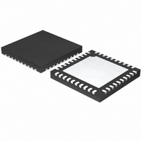
MAX1358BETL+ Maxim Integrated Products, MAX1358BETL+ Datasheet - Page 48

MAX1358BETL+
Manufacturer Part Number
MAX1358BETL+
Description
IC DAS 16BIT 40-TQFN
Manufacturer
Maxim Integrated Products
Type
Data Acquisition System (DAS)r
Datasheet
1.MAX1358BETL.pdf
(71 pages)
Specifications of MAX1358BETL+
Resolution (bits)
16 b
Sampling Rate (per Second)
21.84k
Data Interface
Serial
Voltage Supply Source
Analog and Digital
Voltage - Supply
1.8 V ~ 3.6 V
Operating Temperature
-40°C ~ 85°C
Mounting Type
Surface Mount
Package / Case
40-TQFN Exposed Pad
Number Of Converters
2
Resolution
16 bit
Interface Type
Serial (4-Wire, SPI, QSPI, Microwire)
Voltage Reference
1.25 V
Supply Voltage (max)
3.6 V
Supply Voltage (min)
1.8 V
Maximum Power Dissipation
2051.3 mW
Maximum Operating Temperature
+ 85 C
Mounting Style
SMD/SMT
Input Voltage
1.8 V to 3.6 V
Minimum Operating Temperature
- 40 C
Lead Free Status / RoHS Status
Lead free / RoHS Compliant
The PWM_THTP register contains the bits that set the
PWM on-time and period.
PWMTH<7:0>: PWM time high bits. These bits define
the PWM on (or high)-time and when combined with the
PWMTP<7:0> bits, they determine the duty cycle and
period. The on-time duty cycle is defined as:
To get 50% duty cycle, set PWMTH<7:0> to 126 deci-
mal and PWMTP<7:0> to 253 decimal. Note that setting
PWMTP<7:0> to 255 decimal is not valid as the denom-
inator in the above formula becomes 0. A 100% duty
cycle (i.e., always on) is possible with a value of
PWMTH<7:0> ≥ PWMTP<7:0> > 0. A 0% duty cycle is
possible by setting PWMTH<7:0> = 0 or PWME = 0 in
the PWM_CTRL register. If the PWM is selected to drive
the UPIO_ pin(s), the ALH_ bit(s) (UPIO_CTRL register)
determine the on-time polarity at the beginning of the
PWM cycle. If ALH_ = 1, the on-time at the start of the
PWM period causes a logic-high level (DV
CPOUT) at the UPIO_ pin. When ALH_ = 0, it causes a
logic-low level (DGND) during the on-time. When the
PWM output drives the SWA/B switches, the SWA(B)H
or SWA(B)L bits in the PWM_CTRL register determine
which PWM phase closes these switches. The SPDT1
and SPDT2 switches do not have PWM polarity inver-
sion bits (see the SPDT1<1:0> and SPDT2<1:0> bit
descriptions in the SW_CTRL Register section), but
their effective polarity is set by how the switches are
connected externally. The power-on default is 00 hex.
PWMTP<7:0>: PWM time period bits. These bits con-
trol the PWM output period defined. The PWM output
period is defined as:
Set the PWM input frequency by selecting the
FSEL<2:0> bits as described in Table 14. The power-
on default is 00 hex.
16-Bit, Data-Acquisition System with ADC, DACs,
UPIOs, RTC, Voltage Monitors, and Temp Sensor
PWM_THTP Register (Power-On State: 0000 0000 0000 0000)
48
PWMTH7
PWMTP7
______________________________________________________________________________________
MSB
(PWMTP<7:0> + 1)/(PWM input frequency)
(PWMTH<7:0> + 1)/(PWMTP<7:0> + 1)
PWMTH6
PWMTP6
PWMTH5
PWMTP5
PWMTH4
PWMTP4
DD
or
Writing to the WATCHDOG register address sets the
watchdog timer to 0ms. If the watchdog is enabled
(WDE = 1) and the WATCHDOG register is not written
to before the 750ms expiration, RESET asserts low for
250ms and the watchdog timer restarts at 0ms when
the watchdog timer is enabled. There are no data bits
for this register, and the watchdog timer is reset on the
rising edge of SCLK during the ADR0 bit in the
WATCHDOG register address control byte. Figure 17
shows an example of watchdog timing.
Exit sleep mode and enter normal mode by writing to
the NORM_MD register. The specific normal-mode
state of all circuit blocks is set by the user, who must
configure the individual power-enable bits before enter-
ing sleep mode (Table 15). There are no data bits for
this register, and normal mode begins on the rising
edge of SCLK during the ADR0 bit in the NORM_MD
register address control byte.
Enter sleep mode by writing to the SLEEP register. This
low-power state overrides most of the normal power-
control bits. Table 15 shows which functions are off,
which functions are unaffected (ADE, RTCE, LSDE, and
HYSE), and which functions are controlled by special
sleep-mode bits (SOSCE, SCK32E, and SPWME) while
in sleep mode. There are no data bits for this register,
and sleep mode begins on the rising edge of SCLK
during the ADR0 bit in the SLEEP register address con-
trol byte.
PWMTH3
PWMTP3
WATCHDOG Register (Power-On State: N/A)
NORM_MD Register (Power-On State: N/A)
SLEEP Register (Power-On State: N/A)
PWMTH2
PWMTP2
PWMTH1
PWMTP1
PWMTH0
PWMTP0
LSB


