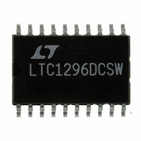
LTC1296DCSW Linear Technology, LTC1296DCSW Datasheet - Page 19

LTC1296DCSW
Manufacturer Part Number
LTC1296DCSW
Description
IC DATA ACQ SYSTEM 12BIT 20-SOIC
Manufacturer
Linear Technology
Type
Data Acquisition System (DAS), ADCr
Datasheet
1.LTC1296CCSWPBF.pdf
(28 pages)
Specifications of LTC1296DCSW
Resolution (bits)
12 b
Sampling Rate (per Second)
46.5k
Data Interface
Serial, Parallel
Voltage Supply Source
Dual ±
Voltage - Supply
±5V
Operating Temperature
0°C ~ 70°C
Mounting Type
Surface Mount
Package / Case
20-SOIC (7.5mm Width)
Lead Free Status / RoHS Status
Contains lead / RoHS non-compliant
Other names
LTC1296DCS
Available stocks
Company
Part Number
Manufacturer
Quantity
Price
Part Number:
LTC1296DCSW
Manufacturer:
LINEAR/凌特
Quantity:
20 000
Company:
Part Number:
LTC1296DCSW#PBF
Manufacturer:
LT
Quantity:
2 122
A
Source Resistance
The analog inputs of the LTC1293/4/6 look like a 100pF
capacitor (C
gets switched between (+) and (–) inputs once during each
conversion cycle. Large external source resistors and
capacitances will slow the settling of the inputs. It is
important that the overall RC time constant is short
enough to allow the analog inputs to settle completely
within the allowed time.
“+” Input Settling
The input capacitor is switched onto the “+” input during
the sample phase (t
2 1/2 CLK cycles before a conversion starts. The voltage on
the “+” input must settle completely within the sample
period. Minimizing R
settling time. If large “+” input source resistance must be
used, the sample time can be increased by using a slower
CLK frequency. With the minimum possible sample time
of 2.5µs R
adequate settling time.
PPLICATI
(+) INPUT
(–) INPUT
D
SOURCE
CLK
D
OUT
CS
IN
IN
) in series with a 500Ω resistor (R
O
+ < 1.5kΩ Ω Ω Ω Ω and C1 < 20pF will provide
SMPL
U
SOURCE
S
, see Figure 8). The sample period
I FOR ATIO
U
+ and C1 will improve the
START
HI-Z
W
Figure 8. “+” and “–” Input Settling Windows
SGL/
DIFF
U
ON
). C
SAMPLE
IN
(+) INPUT MUST SETTLE DURING THIS TIME
“–” Input Settling
At the end of the sample phase the input capacitor switches
to the “-” input and the conversion starts (see Figure 8).
During the conversion, the “+” input voltage is effectively
“held” by the sample and hold and will not affect the
conversion result. It is critical that the “–” input voltage be
free of noise and settle completely during the first CLK
cycle of the conversion. Minimizing R
improve settling time. If large “–” input source resistance
must be used the time can be extended by using a slower
CLK frequency. At the maximum CLK frequency of 1MHz,
R
settling.
Input Op Amps
When driving the analog inputs with an op amp it is
important that the op amp settles within the allowed time
(see Figure 8). Again the “+” and “–” input sampling times
can be extended as described above to accommodate
slower op amps. Most op amps including the LT1006 and
LT1013 single supply op amps can be made to settle
SOURCE
MSBF
1ST BIT TEST (–) INPUT MUST
LTC1293/LTC1294/LTC1296
– < 250Ω Ω Ω Ω Ω and C2 < 20pF will provide adequate
t
SETTLE DURING THIS TIME
SMPL
PS
HOLD
SOURCE
B11
LTC1293 F08
– and C2 will
19
129346fs


