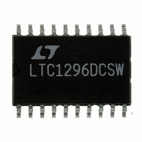
LTC1296DCSW Linear Technology, LTC1296DCSW Datasheet - Page 7

LTC1296DCSW
Manufacturer Part Number
LTC1296DCSW
Description
IC DATA ACQ SYSTEM 12BIT 20-SOIC
Manufacturer
Linear Technology
Type
Data Acquisition System (DAS), ADCr
Datasheet
1.LTC1296CCSWPBF.pdf
(28 pages)
Specifications of LTC1296DCSW
Resolution (bits)
12 b
Sampling Rate (per Second)
46.5k
Data Interface
Serial, Parallel
Voltage Supply Source
Dual ±
Voltage - Supply
±5V
Operating Temperature
0°C ~ 70°C
Mounting Type
Surface Mount
Package / Case
20-SOIC (7.5mm Width)
Lead Free Status / RoHS Status
Contains lead / RoHS non-compliant
Other names
LTC1296DCS
Available stocks
Company
Part Number
Manufacturer
Quantity
Price
Part Number:
LTC1296DCSW
Manufacturer:
LINEAR/凌特
Quantity:
20 000
Company:
Part Number:
LTC1296DCSW#PBF
Manufacturer:
LT
Quantity:
2 122
LTC1293
LTC1294
LTC1296
PI FU CTIO S
#
1 –8
9
10
11
12
13, 14 REF
15
16
17
18
19, 20 AV
#
1 –8
9
10
11
12
13, 14 REF
15
16
17
18
19
20
#
1 – 6
7
8
9
10
11
12
13
14
15
16
U
PIN
CH0 – CH7
COM
DGND
V
AGND
D
D
CS
CLK
PIN
CH0 – CH7
COM
DGND
V
AGND
D
D
CS
CLK
SSO
V
PIN
CH0 – CH5
COM
DGND
V
AGND
V
D
D
CS
CLK
V
CC
REF
CC
–
IN
OUT
–
IN
OUT
–
IN
OUT
CC,
–
–
, REF
, REF
U
DV
CC
+
+
FUNCTION
Analog Inputs
Common
Digital Ground
Negative Supply
Analog Ground
Ref. Inputs
Data Input
Digital Data Output The A/D conversion result is shifted out of this output.
Chip Select Input
Clock
Positive Supplies
FUNCTION
Analog Inputs
Common
Digital Ground
Negative Supply
Analog Ground
Ref. Inputs
Data Input
Digital Data Output The A/D conversion result is shifted out of this output.
Chip Select Input
Clock
System Shutdown
Output
Positive Supply
FUNCTION
Analog Inputs
Common
Digital Ground
Negative Supply
Analog Ground
Ref. Input
Data Input
Digital Data Output The A/D conversion result is shifted out of this output.
Chip Select Input
Clock
Positive supply
U
DESCRIPTION
The analog inputs must be free of noise with respect to AGND.
The common pin defines the zero reference point for all single ended inputs. It must be free of noise and is
usually tied to the analog ground plane.
This is the ground for the internal logic. Tie to the ground plane.
Tie V
AGND should be tied directly to the analog ground plane.
The reference inputs must be kept free of noise with respect to AGND.
The A/D configuration word is shifted into this input.
A logic low on this input enables data transfer.
This clock synchronizes the serial data transfer and controls A/D conversion rate.
This supply must be kept free of noise and ripple by bypassing directly to the analog ground plane.
DESCRIPTION
The analog inputs must be free of noise with respect to AGND.
The common pin defines the zero reference point for all single ended inputs. It must be free of noise and is
usually tied to the analog ground plane.
This is the ground for the internal logic. Tie to the ground plane.
Tie V
AGND should be tied directly to the analog ground plane.
The reference inputs must be kept free of noise with respect to AGND. The A/D sees a reference voltage equal
to the difference between REF
The A/D configuration word is shifted into this input.
A logic low on this input enables data transfer.
This clock synchronizes the serial data transfer and controls A/D converion rate.
These supplies must be kept free of noise and ripple by bypassing directly to the analog ground plane. AV
and DV
DESCRIPTION
The analog inputs must be free of noise with respect to AGND.
The common pin defines the zero reference point for all single ended inputs. It must be free of noise and is
usually tied to the analog ground plane.
This is the ground for the internal logic. Tie to the ground plane.
Tie V
AGND should be tied directly to the analog ground plane.
The reference inputs must be kept free of noise with respect to AGND. The A/D sees a reference voltage equal
to the difference between REF
The A/D configuration word is shifted into this input.
A logic low on this input enables data transfer.
This clock synchronizes the serial data transfer and controls A/D conversion rate.
System Shutdown Output pin will go low when power shutdown is requested.
This supply must be kept free of noise and ripple by bypassing directly to the analog ground plane.
–
–
–
to most negative potential in the circuit (Ground in single supply applications).
to most negative potential in the circuit (Ground in single supply applications).
to most negative potential in the circuit (Ground in single supply applications).
CC
must be tied together.
+
+
and REF
and REF
–
–
.
.
LTC1293/LTC1294/LTC1296
129346fs
CC
7


