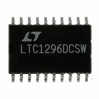
LTC1296DCSW Linear Technology, LTC1296DCSW Datasheet - Page 22

LTC1296DCSW
Manufacturer Part Number
LTC1296DCSW
Description
IC DATA ACQ SYSTEM 12BIT 20-SOIC
Manufacturer
Linear Technology
Type
Data Acquisition System (DAS), ADCr
Datasheet
1.LTC1296CCSWPBF.pdf
(28 pages)
Specifications of LTC1296DCSW
Resolution (bits)
12 b
Sampling Rate (per Second)
46.5k
Data Interface
Serial, Parallel
Voltage Supply Source
Dual ±
Voltage - Supply
±5V
Operating Temperature
0°C ~ 70°C
Mounting Type
Surface Mount
Package / Case
20-SOIC (7.5mm Width)
Lead Free Status / RoHS Status
Contains lead / RoHS non-compliant
Other names
LTC1296DCS
Available stocks
Company
Part Number
Manufacturer
Quantity
Price
Part Number:
LTC1296DCSW
Manufacturer:
LINEAR/凌特
Quantity:
20 000
Company:
Part Number:
LTC1296DCSW#PBF
Manufacturer:
LT
Quantity:
2 122
A
a 1.25 reference. If this offset is unacceptable, it can be
corrected digitally by the receiving system or by offsetting
the “–” input to the LTC1293/4/6.
Noise with Reduced V
The total input referred noise of the LTC1293/4/6 can be
reduced to approximately 200µV peak-to-peak using a
ground plane, good bypassing, good layout techniques
and minimizing noise on the reference inputs. This noise
is insignificant with a 5V reference input but will become
a larger fraction of an LSB as the size of the LSB is reduced.
The typical performance characteristic curve of Noise
Error vs Reference Voltage shows the LSB contribution of
this 200µV of noise.
For operation with a 5V reference, the 200µV noise is only
0.16LSB peak-to-peak. Here the LTC1293/4/6 noise will
contribute virtually no uncertainty to the output code. For
reduced references, the noise may become a significant
fraction of an LSB and cause undesirable jitter in the
output code. For example, with a 1.25V reference, this
200µV noise is 0.64LSB peak-to-peak. This will reduce
the range of input voltages over which a stable output code
can be achieved by 0.64LSB. Now averaging readings may
be necessary.
This noise data was taken in a very clean test fixture. Any
setup induced noise (noise or ripple on V
will add to the internal noise. The lower the reference
voltage used, the more critical it becomes to have a noise-
free setup.
Gain Error due to Reduced V
The gain error of the LTC1294/6 is very good over a wide
range of reference voltages. The error component that is
seen in the typical performance characteristics curve
Change in Gain Error vs Reference Voltage for the LTC1293
is due the voltage drop on the AGND pin from the device
to the ground plane. To minimize this error the LTC1293
should be soldered directly onto the PC board. The internal
reference point for V
in the AGND pin will make the reference voltage, internal
to the device, less than what is applied externally (Figure
15). This drop is typically 400µV due to the product of the
pin resistance (R
LTC1293/LTC1294/LTC1296
22
PPLICATI
O
PIN
) and the LTC1293 supply current. For
U
REF
S
REF
is tied to AGND. Any voltage drop
I FOR ATIO
U
REF
W
CC
, V
REF
U
or V
IN
)
example, with V
change of –1.0LSB from the gain error measured with
V
LTC1293/4/6 AC Characteristics
Two commonly used figures of merit for specifying the
dynamic performance of the A/Ds in digital signal process-
ing applications are the Signal-to-Noise Ratio (SNR) and
the “effective number of bits”(ENOB). SNR is the ratio of
the RMS magnitude of the fundamental to the RMS
magnitude of all the non-fundamental signals up to the
Nyquist frequency (half the sampling frequency). The
theoretical maximum SNR for a sine wave input is given
by:
where N is the number of bits. Thus the SNR depends on
the resolution of the A/D. For an ideal 12-bit A/D the SNR
is equal to 74dB. A Fast Fourier Transform (FFT) plot of the
output spectrum of the LTC1294 is shown in Figures 16a
and 16b. The input (f
with the sampling frequency (f
obtained from the plot are 72.7dB and 72.5dB.
Rewriting the SNR expression it is possible to obtain the
equivalent resolution based on the SNR measurement.
This is the so-called effective number of bits (ENOB). For
the example shown in Figures 16a and 16b, N = 11.8 bits.
Figure 17 shows a plot of ENOB as a function of input
frequency. The top curve shows the A/D’s ENOB remains
at 11.8 for input frequencies up to f
REF
SNR = (6.02N + 1.76dB)
N
= 5V.
=
⎛
⎜
⎝
SNR
Figure 15. Parasitic Pin Resistance (R
I
CC
AGND
6 02
– .
.
REF
1 76
R
PIN
= 1.25V this will result in a gain error
dB
IN
REF
LTC1293
) frequencies are 1kHz and 22kHz
⎞
⎟
⎠
DAC
–
REF
+
S
V
) at 45.4kHz. The SNR
REF
±
S
/2 with ±5V supplies.
REFERENCE
VOLTAGE
LTC1293 F15
PIN
)
129346fs


