CAT5114ZD7I10GT3 ON Semiconductor, CAT5114ZD7I10GT3 Datasheet - Page 5
CAT5114ZD7I10GT3
Manufacturer Part Number
CAT5114ZD7I10GT3
Description
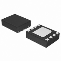
IC POT DIGITAL 10K 32TAP 8TDFN
Manufacturer
ON Semiconductor
Datasheet
1.CAT5114ZD7I10GT3.pdf
(15 pages)
Specifications of CAT5114ZD7I10GT3
Taps
32
Resistance (ohms)
10K
Number Of Circuits
1
Temperature Coefficient
300 ppm/°C Typical
Memory Type
Non-Volatile
Interface
Up/Down
Voltage - Supply
2.5 V ~ 6 V
Operating Temperature
-40°C ~ 85°C
Mounting Type
Surface Mount
Package / Case
8-VFDFN Exposed Pad
Resistance In Ohms
10K
Number Of Pots
Single
Taps Per Pot
32
Resistance
10 KOhms
Wiper Memory
Non Volatile
Digital Interface
Serial (3-Wire)
Operating Supply Voltage
3.3 V or 5 V
Supply Current
0.1 mA
Maximum Operating Temperature
+ 85 C
Minimum Operating Temperature
- 40 C
Mounting Style
SMD/SMT
Supply Voltage (max)
6 V
Supply Voltage (min)
2.5 V
Lead Free Status / RoHS Status
Lead free / RoHS Compliant
Other names
CAT5114ZD7I-10-G
CAT5114ZD7I-10-GT3TR
CAT5114ZD7I-10-GT3TR
CAT5114ZD7I-10-GTR
CAT5114ZD7I-10-GTR
CAT5114ZD7I10GT3TR
CAT5114ZD7I-10-GT3TR
CAT5114ZD7I-10-GT3TR
CAT5114ZD7I-10-GTR
CAT5114ZD7I-10-GTR
CAT5114ZD7I10GT3TR


3. This parameter is tested initially and after a design or process change that affects the parameter.
4. Latch−up protection is provided for stresses up to 100 mA on address and data pins from −1 V to V
5. I
6. These parameters are periodically sampled and are not 100% tested.
Table 5. DC ELECTRICAL CHARACTERISTICS
POWER SUPPLY
LOGIC INPUTS
POTENTIOMETER CHARACTERISTICS
I
SB1
C
W
Symbol
TC
TC
H
= source or sink.
R
I
I
V
V
V
DNL
/C
(Note 4)
V
CC1
CC2
V
R
INL
I
I
V
I
RATIO
CC
IH
IH2
POT
RPOT
IL
IL2
fc
RH
W
RL
WI
N
L
/C
W
Operating Voltage Range
Supply Current (Increment)
Supply Current (Write)
Supply Current (Standby)
Input Leakage Current
Input Leakage Current
CMOS High Level Input Voltage
CMOS Low Level Input Voltage
Potentiometer Resistance
Pot. Resistance Tolerance
Voltage on R
Voltage on R
Resolution
Integral Linearity Error
Differential Linearity Error
Wiper Resistance
Wiper Current
TC of Pot Resistance
Ratiometric TC
Noise
Potentiometer Capacitances
Frequency Response
Parameter
H
L
pin
pin
V
V
Programming, V
V
CS = V
U/D, INC = V
V
V
2.5 V ≤ V
−10 Device
−50 Device
−00 Device
I
I
V
V
100 kHz / 1 kHz
Passive Attenuator, 10 kW
W
W
(V
CC
CC
CC
IN
IN
CC
CC
http://onsemi.com
≤ 2 mA
≤ 2 mA
CC
= V
= 0 V
= 6 V, f = 1 MHz, I
= 6 V, f = 250 kHz, I
= 3 V
= 5 V, I
= 2.5 V, I
= +2.5 V to +6 V unless otherwise specified)
CC
CC
CC
Conditions
− 0.3 V
W
≤ 6 V
5
CC
W
= 1 mA
= 1 mA
CC
− 0.3 V or GND
= 6 V
W
W
= 0
= 0
V
CC
−0.3
Min
−4.4
2.5
–
–
–
–
–
–
–
0
0
x 0.7
CC
+ 1 V.
8/8/25
Typ
0.25
8/24
100
150
300
3.2
0.5
1.7
10
50
70
–
–
–
–
–
−
–
–
–
–
V
V
CC
CC
1000
Max
100
500
−10
V
V
6.0
±20
200
400
50
10
0.5
4.4
20
1
1
+ 0.3
CC
CC
x 0.2
ppm/°C
ppm/°C
nV/√Hz
Units
MHz
LSB
LSB
mA
mA
mA
mA
mA
mA
mA
mA
kW
pF
V
V
V
%
%
W
W
V
V
Related parts for CAT5114ZD7I10GT3
Image
Part Number
Description
Manufacturer
Datasheet
Request
R

Part Number:
Description:
32-Tap Digitally Programmable Potentiometer (DPP)
Manufacturer:
Catalyst Semiconductor
Datasheet:

Part Number:
Description:
ON Semiconductor [VOLTAGE REGULATOR]
Manufacturer:
ON Semiconductor
Datasheet:
Part Number:
Description:
357-036-542-201 CARDEDGE 36POS DL .156 BLK LOPRO
Manufacturer:
ON Semiconductor
Datasheet:
Part Number:
Description:
357-036-542-201 CARDEDGE 36POS DL .156 BLK LOPRO
Manufacturer:
ON Semiconductor
Datasheet:
Part Number:
Description:
357-036-542-201 CARDEDGE 36POS DL .156 BLK LOPRO
Manufacturer:
ON Semiconductor
Datasheet:
Part Number:
Description:
357-036-542-201 CARDEDGE 36POS DL .156 BLK LOPRO
Manufacturer:
ON Semiconductor
Datasheet:
Part Number:
Description:
357-036-542-201 CARDEDGE 36POS DL .156 BLK LOPRO
Manufacturer:
ON Semiconductor
Datasheet:
Part Number:
Description:
357-036-542-201 CARDEDGE 36POS DL .156 BLK LOPRO
Manufacturer:
ON Semiconductor
Datasheet:
Part Number:
Description:
357-036-542-201 CARDEDGE 36POS DL .156 BLK LOPRO
Manufacturer:
ON Semiconductor
Datasheet:
Part Number:
Description:
357-036-542-201 CARDEDGE 36POS DL .156 BLK LOPRO
Manufacturer:
ON Semiconductor
Datasheet:
Part Number:
Description:
357-036-542-201 CARDEDGE 36POS DL .156 BLK LOPRO
Manufacturer:
ON Semiconductor
Datasheet:
Part Number:
Description:
357-036-542-201 CARDEDGE 36POS DL .156 BLK LOPRO
Manufacturer:
ON Semiconductor
Datasheet:
Part Number:
Description:
Manufacturer:
ON Semiconductor
Datasheet:
Part Number:
Description:
Manufacturer:
ON Semiconductor
Datasheet: