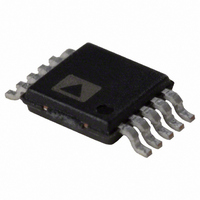
AD5272BRMZ-20 Analog Devices Inc, AD5272BRMZ-20 Datasheet - Page 20

AD5272BRMZ-20
Manufacturer Part Number
AD5272BRMZ-20
Description
IC DGTL POT 20K 1024POS 10MSOP
Manufacturer
Analog Devices Inc
Datasheet
1.AD5274BRMZ-20.pdf
(28 pages)
Specifications of AD5272BRMZ-20
Design Resources
Compact, Low Cost, 5 V, Variable Gain, Noninverting Amplifier Using AD5270/2 and AD8615 (CN0161) Compact, Low Cost, 5 V, Variable Gain, Inverting Amplifier Using AD5270/2 and AD8615(CN0168)
Taps
1024
Resistance (ohms)
20K
Number Of Circuits
1
Temperature Coefficient
5ppm/°C
Memory Type
Non-Volatile
Interface
I²C, 2-Wire Serial
Voltage - Supply
2.7 V ~ 5.5 V, ±2.5 V ~ 2.75 V
Operating Temperature
-40°C ~ 125°C
Mounting Type
Surface Mount
Package / Case
10-MSOP, Micro10™, 10-uMAX, 10-uSOP
Resistance In Ohms
*
End To End Resistance
20kohm
Track Taper
Linear
Resistance Tolerance
± 1%
No. Of Steps
1024
Supply Voltage Range
2.7V To 5.5V
Control Interface
I2C, Serial
No. Of Pots
Single
Lead Free Status / RoHS Status
Lead free / RoHS Compliant
Available stocks
Company
Part Number
Manufacturer
Quantity
Price
Company:
Part Number:
AD5272BRMZ-20
Manufacturer:
AD
Quantity:
1 001
Part Number:
AD5272BRMZ-20
Manufacturer:
ADI/亚德诺
Quantity:
20 000
AD5272/AD5274
READ OPERATION
When reading data back from the AD5272/AD5274, the user
must first issue a readback command to the device, this begins
with a start command followed by an address byte (R/ W = 0),
after which the AD5272/AD5274 acknowledges that it is
prepared to receive data by pulling SDA low.
Two bytes of data are then written to the AD5272/AD5274, the
most significant byte followed by the least significant byte; both
of these data bytes are acknowledged by the AD5272/AD5274.
SDA
SDA
SCL
SCL
START BY
START BY
MASTER
MASTER
0
1
0
1
1
1
SERIAL BUS ADDRESS BYTE
SERIAL BUS ADDRESS BYTE
0
0
SDA (CONTINUED)
SDA (CONTINUED)
SCL (CONTINUED)
SCL (CONTINUED)
FRAME 1
FRAME 1
1
1
1
1
A1
A1
A0
A0
Figure 45. Read Command
AD5272/AD5274
R/W
R/W
9
Rev. C | Page 20 of 28
9
ACK. BY
ACK. BY
AD5272/AD5274
D7
1
D7
9
1
9
D6
1
0
D6
0
1
A stop condition follows. These bytes contain the read instruc-
tion, which enables readback of the RDAC register, 50-TP
memory, or the control register. The user can then read back
the data beginning with a start command followed by an
address byte (R/ W = 1), after which the device acknowledges
that it is prepared to transmit data by pulling SDA low. Two
bytes of data are then read from the device, as shown in
A stop condition follows. If the master does not acknowledge
the first byte, the second byte is not transmitted by the
AD5272/AD5274.
LEAST SIGNIFICANT DATA BYTE
LEAST SIGNIFICANT DATA BYTE
D5
0
D5
0
D4
X
C3
MOST SIGNIFICANT DATA BYTE
D4
MOST SIGNIFICANT DATA BYTE
FRAME 3
FRAME 3
D3
X
C2
D3
FRAME 2
FRAME 2
D2
X
C1
D2
D1
X
C0
D1
AD5272/AD5274
D9
D0
D9
D0
ACK. BY
NO ACK. BY
MASTER
D8
9
D8
9
ACK. BY
MASTER
ACK. BY
AD5272/AD5274
STOP BY
MASTER
STOP BY
MASTER
9
9
Figure 45
.


