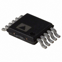
AD5304BRMZ Analog Devices Inc, AD5304BRMZ Datasheet

AD5304BRMZ
Specifications of AD5304BRMZ
Available stocks
Related parts for AD5304BRMZ
AD5304BRMZ Summary of contents
Page 1
FEATURES AD5304: 4 buffered 8-Bit DACs in 10-lead MSOP and 10-lead LFCSP A Version: ±1 LSB INL, B Version: ±0.625 LSB INL AD5314: 4 buffered 10-Bit DACs in 10-lead MSOP and 10-lead LFCSP A Version: ±4 LSB INL, B Version: ...
Page 2
AD5304/AD5314/AD5324 TABLE OF CONTENTS Features .............................................................................................. 1 Applications....................................................................................... 1 General Description ......................................................................... 1 Functional Block Diagram .............................................................. 1 Revision History ............................................................................... 2 Specifications..................................................................................... 3 AC Characteristics........................................................................ 4 Timing Characteristics ................................................................ 5 Absolute Maximum Ratings............................................................ 6 ESD Caution.................................................................................. 6 Pin Configurations ...
Page 3
SPECIFICATIONS kΩ to GND REF L Table 1. Parameter 1 Min PERFORMANCE AD5304 Resolution Relative Accuracy Differential Nonlinearity AD5314 Resolution Relative ...
Page 4
AD5304/AD5314/AD5324 1 Parameter Min 5 LOGIC INPUTS Input Current V , Input Low Voltage Input High Voltage 2.4 IH 2.1 2.0 Pin Capacitance POWER REQUIREMENTS V 2 (Normal Mode 4.5 V ...
Page 5
TIMING CHARACTERISTICS 5.5 V; all specifications T DD Table 3. Limit Parameter ...
Page 6
AD5304/AD5314/AD5324 ABSOLUTE MAXIMUM RATINGS T = 25°C, unless otherwise noted. A Table 4. 1 Parameter Rating V to GND –0 Digital Input Voltage to GND –0 Reference Input Voltage to GND –0.3 ...
Page 7
PIN CONFIGURATIONS AND FUNCTION DESCRIPTIONS AD5304 OUT AD5314 AD5324 OUT TOP VIEW OUT (Not to Scale) REFIN 5 Figure 3. MSOP Pin Configuration Table 5. Pin Function Descriptions ...
Page 8
AD5304/AD5314/AD5324 TYPICAL PERFORMANCE CHARACTERISTICS 1 25° 0.5 0 –0.5 –1 100 150 CODE Figure 5. AD5304 Typical INL Plot 25° ...
Page 9
T = 25° MAX INL 0.25 MAX DNL 0 MIN DNL –0.25 MIN INL –0. (V) REF Figure 11. AD5304 INL and DNL Error vs ...
Page 10
AD5304/AD5314/AD5324 600 –40°C 500 +25°C 400 +105°C 300 200 100 0 2.5 3.0 3.5 4.0 V (V) DD Figure 17. Supply Current vs. Supply Voltage 0.5 0.4 0.3 0.2 +25°C 0.1 0 2.5 3.0 3.5 4.0 V (V) DD Figure ...
Page 11
300 350 400 450 500 I (µA) DD Figure 23. I Histogram with and 2.50 2.49 2.48 2.47 1µs/DIV Figure 24. AD5324 Major-Code Transition Glitch Energy 10 0 –10 ...
Page 12
AD5304/AD5314/AD5324 TERMINOLOGY Relative Accuracy or Integral Nonlinearity (INL) For the DAC, relative accuracy or integral nonlinearity (INL measure of the maximum deviation, in LSB, from a straight line passing through the endpoints of the DAC transfer function. Typical ...
Page 13
OUTPUT IDEAL VOLTAGE ACTUAL NEGATIVE OFFSET DAC CODE ERROR DEAD BAND CODES AMPLIFIER FOOTROOM (1mV) NEGATIVE OFFSET ERROR Figure 28. Transfer Function with Negative Offset GAIN ERROR PLUS OFFSET ERROR ACTUAL OUTPUT VOLTAGE POSITIVE OFFSET Figure 29. Transfer Function with ...
Page 14
AD5304/AD5314/AD5324 THEORY OF OPERATION FUNCTIONAL DESCRIPTION The AD5304/AD5314/AD5324 are quad, resistor-string DACs fabricated on a CMOS process with resolutions of 8, 10, and 12 bits, respectively. Each contains four output buffer amplifiers and is written to via a 3-wire serial ...
Page 15
BIT15 (MSB) A1 BIT15 (MSB) A1 BIT15 (MSB) A1 Input Shift Register The input shift register is 16 bits wide. Data is loaded into the device as a 16-bit word under the control of a serial clock input, SCLK. See ...
Page 16
AD5304/AD5314/AD5324 Double-Buffered Interface The AD5304/AD5314/AD5324 DACs have double-buffered inter- faces consisting of two banks of registers—input registers and DAC registers. The input register is directly connected to the input shift register and the digital code is transferred to the rele- ...
Page 17
AD5304/AD5314/AD5324 to 68HC11/68L11 Interface Figure 37 shows a serial interface between the AD5304/AD5314/ AD5324 and the 68HC11/68L11 microcontroller. SCK of the 68HC11/68L11 drives the SCLK of the AD5304/AD5314/ AD5324, while the MOSI output drives the serial data line (DIN) of ...
Page 18
AD5304/AD5314/AD5324 APPLICATIONS TYPICAL APPLICATION CIRCUIT The AD5304/AD5314/AD5324 can be used with a wide range of reference voltages where the devices offer full, one-quadrant multiplying capability over a reference range More typically, these devices are used ...
Page 19
Opto-Isolated Interface for Process Control Applications The AD5304/AD5314/AD5324 have a versatile 3-wire serial inter-face, making them ideal for generating accurate voltages in process control and industrial applications. Due to noise, safety requirements, or distance, it might be necessary to iso- ...
Page 20
AD5304/AD5314/AD5324 POWER SUPPLY BYPASSING AND GROUNDING In any circuit where accuracy is important, careful consider- ation of the power supply and ground return layout helps to ensure the rated performance. The printed circuit board on which the AD5304/AD5314/AD5324 is mounted ...
Page 21
Table 8. Overview of AD53xx Parallel Devices Part No. Resolution DNL SINGLES AD5330 8 ±0.25 AD5331 10 ±0.5 AD5340 12 ±1.0 AD5341 12 ±1.0 DUALS AD5332 8 ±0.25 AD5333 10 ±0.5 AD5342 12 ±1.0 AD5343 12 ±1.0 QUADS AD5334 8 ...
Page 22
AD5304/AD5314/AD5324 OUTLINE DIMENSIONS 3.10 3.00 2. 5.15 3.10 4.90 3.00 4.65 2. PIN 1 0.50 BSC 0.95 0.85 1.10 MAX 0.75 0.15 0.33 SEATING 0.23 0.05 PLANE 0.17 0.08 COPLANARITY 0.10 COMPLIANT TO JEDEC STANDARDS MO-187-BA ...
Page 23
... AD5304BRM-REEL –40°C to +105°C AD5304BRM-REEL7 –40°C to +105°C 1 AD5304BRMZ –40°C to +105°C AD5304BRMZ-REEL 1 –40°C to +105°C 1 AD5304BRMZ-REEL7 –40°C to +105°C 1 AD5304BCPZ-REEL7 –40°C to +105°C 1 AD5314ACPZ-REEL7 –40°C to +105°C AD5314ARM –40°C to +105°C AD5314ARM-REEL7 – ...
Page 24
AD5304/AD5314/AD5324 NOTES ©2006 Analog Devices, Inc. All rights reserved. Trademarks and registered trademarks are the property of their respective owners. C00929-0-9/06(F) Rev Page ...


