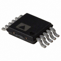
AD5664RBRMZ-3 Analog Devices Inc, AD5664RBRMZ-3 Datasheet - Page 16

AD5664RBRMZ-3
Manufacturer Part Number
AD5664RBRMZ-3
Description
IC DAC NANO 16BIT 1.25V 10-MSOP
Manufacturer
Analog Devices Inc
Series
nanoDAC™r
Specifications of AD5664RBRMZ-3
Data Interface
Serial
Settling Time
4µs
Number Of Bits
16
Number Of Converters
4
Voltage Supply Source
Single Supply
Power Dissipation (max)
6.6mW
Operating Temperature
-40°C ~ 105°C
Mounting Type
Surface Mount
Package / Case
10-MSOP, Micro10™, 10-uMAX, 10-uSOP
Resolution (bits)
16bit
Sampling Rate
220kSPS
Input Channel Type
Serial
Supply Current
950µA
Digital Ic Case Style
SOP
No. Of Pins
10
Lead Free Status / RoHS Status
Lead free / RoHS Compliant
For Use With
EVAL-AD5664REBZ - BOARD EVALUATION FOR AD5664R
Lead Free Status / RoHS Status
Lead free / RoHS Compliant, Lead free / RoHS Compliant
Available stocks
Company
Part Number
Manufacturer
Quantity
Price
Part Number:
AD5664RBRMZ-3
Manufacturer:
ADI/亚德诺
Quantity:
20 000
AD5624/AD5664
INPUT SHIFT REGISTER
The input shift register is 24 bits wide The first two bits are
don’t care bits. The next three bits are the Command bits, C2 to
C0 (see Table 7), followed by the 3-bit DAC address, A2 to A0
(see Table 8), and then the 16-, 12-bit data-word. The data-word
comprises the 16-, 12- bit input code followed by 0 or 4 don’t
care bits for the AD5664 and AD5624 respectively (see Figure
31 and Figure 32). These data bits are transferred to the DAC
register on the 24
Table 7. Command Definition
C2
0
0
0
0
1
1
1
1
Table 8. Address Command
A2
0
0
0
0
1
SCLK
SYNC
DIN
C1
0
0
1
1
0
0
1
1
A1
0
0
1
1
1
DB23 (MSB)
DB23 (MSB)
SYNC HIGH BEFORE 24
C0
0
1
0
1
0
1
0
1
X
X
DB23
th
INVALID WRITE SEQUENCE:
X
X
falling edge of SCLK.
Command
Write to input register n
Update DAC register n
Write to input register n, update all
(software LDAC)
Write to and update DAC channel n
Power down DAC (power-up)
Reset
Load LDAC register
Reserved
COMMAND BITS
COMMAND BITS
C2
C2
A0
0
1
0
1
1
C1
C1
TH
C0
C0
FALLING EDGE
ADDRESS (n)
DAC A
DAC B
DAC C
DAC D
All DACs
ADDRESS BITS
ADDRESS BITS
A2
A2
DB0
A1
A1
A0
A0
Figure 31. AD5664 Input Shift Register Contents
Figure 32. AD5624 Input Shift Register Contents
D15
D11
D14
D10
Figure 33. SYNC Interrupt Facility
D13
D9
Rev. 0 | Page 16 of 24
D12
D8
D11
D7
DATA BITS
D10
D6
SYNC INTERRUPT
In a normal write sequence, the SYNC line is kept low for at least
24 falling edges of SCLK, and the DAC is updated on the 24
falling edge. However, if SYNC is brought high before the 24
falling edge, then this acts as an interrupt to the write sequence.
The input shift register is reset and the write sequence is seen as
invalid. Neither an update of the DAC register contents nor a
change in the operating mode occurs (see Figure 33).
POWER-ON RESET
The AD5624/AD5664 family contains a power-on reset circuit
that controls the output voltage during power-up. The AD5624/
AD5664 DAC outputs power up to 0 V and the output remains
there until a valid write sequence is made to the DAC. This is
useful in applications where it is important to know the state of
the output of the DAC while it is in the process of powering up.
D9
D5
VALID WRITE SEQUENCE, OUTPUT UPDATES
D8
D4
DATA BITS
DB23
ON THE 24
D7
D3
D6
D2
TH
D5
D1
FALLING EDGE
D4
D0
D3
X
DB0
D2
X
D1
DB0 (LSB)
DB0 (LSB)
X
D0
X
th
th


