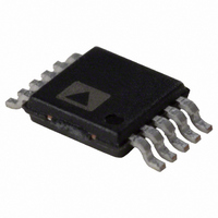
AD5664RBRMZ-3 Analog Devices Inc, AD5664RBRMZ-3 Datasheet - Page 19

AD5664RBRMZ-3
Manufacturer Part Number
AD5664RBRMZ-3
Description
IC DAC NANO 16BIT 1.25V 10-MSOP
Manufacturer
Analog Devices Inc
Series
nanoDAC™r
Specifications of AD5664RBRMZ-3
Data Interface
Serial
Settling Time
4µs
Number Of Bits
16
Number Of Converters
4
Voltage Supply Source
Single Supply
Power Dissipation (max)
6.6mW
Operating Temperature
-40°C ~ 105°C
Mounting Type
Surface Mount
Package / Case
10-MSOP, Micro10™, 10-uMAX, 10-uSOP
Resolution (bits)
16bit
Sampling Rate
220kSPS
Input Channel Type
Serial
Supply Current
950µA
Digital Ic Case Style
SOP
No. Of Pins
10
Lead Free Status / RoHS Status
Lead free / RoHS Compliant
For Use With
EVAL-AD5664REBZ - BOARD EVALUATION FOR AD5664R
Lead Free Status / RoHS Status
Lead free / RoHS Compliant, Lead free / RoHS Compliant
Available stocks
Company
Part Number
Manufacturer
Quantity
Price
Part Number:
AD5664RBRMZ-3
Manufacturer:
ADI/亚德诺
Quantity:
20 000
MICROPROCESSOR INTERFACING
AD5624/AD5664 to Blackfin® ADSP-BF53x Interface
Figure 35
the Blackfin ADSP-BF53x microprocessor. The ADSP-BF53x
processor family incorporates two dual-channel synchronous serial
ports, SPORT1 and SPORT0, for serial and multiprocessor commu-
nications. Using SPORT0 to connect to the AD5624/AD5664, the
setup for the interface is as follows. DTOPRI drives the DIN pin of
the AD5624/AD5664, while TSCLK0 drives the SCLK of the part.
The
AD5624/AD5664 to 68HC11/68L11 Interface
Figure 36 shows a serial interface between the AD5624/AD5664
and the 68HC11/68L11 microcontroller. SCK of the 68HC11/
68L11 drives the SCLK of the AD5624/AD5664, while the
MOSI output drives the serial data line of the DAC.
The SYNC signal is derived from a port line (PC7). The setup
conditions for correct operation of this interface are as follows.
The 68HC11/68L11 is configured with its CPOL bit as a 0 and
its CPHA bit as a 1. When data is being transmitted to the DAC,
the SYNC line is taken low (PC7). When the 68HC11/68L11 is
configured as described previously, data appearing on the MOSI
output is valid on the falling edge of SCK. Serial data from the
68HC11/68L11 is transmitted in 10-bit bytes with only eight
falling clock edges occurring in the transmit cycle. Data is
transmitted MSB first. To load data to the AD5624/AD5664,
PC7 is left low after the first eight bits are transferred, and a
second serial write operation is performed to the DAC; PC7 is
taken high at the end of this procedure.
SYNC
Figure 35. Blackfin ADSP-BF53x Interface to AD5624/AD5664
Figure 36. 68HC11/68L11 Interface to AD5624/AD5664
shows a serial interface between the AD5624/AD5664 and
is driven from TFS0.
1
1
ADDITIONAL PINS OMITTED FOR CLARITY.
68HC11/68L11
ADDITIONAL PINS OMITTED FOR CLARITY.
ADSP-BF53x
TSCLK0
DTOPRI
TFS0
MOSI
SCK
PC7
1
1
SYNC
DIN
SCLK
SYNC
SCLK
DIN
AD5664
AD5624/
AD5664
AD5624/
1
1
Rev. 0 | Page 19 of 24
AD5624/AD5664 to 80C51/80L51 Interface
Figure 37 shows a serial interface between the AD5624/AD5664
and the 80C51/80L51 microcontroller. The setup for the interface
is as follows. TxD of the 80C51/80L51 drives SCLK of the
AD5624/AD5664, while RxD drives the serial data line of the
part. The SYNC signal is derived from a bit-programmable pin
on the port. In this case, port line P3.3 is used. When data is
transmitted to the AD5624/AD5664, P3.3 is taken low. The
80C51/80L51 transmits data in 10-bit bytes only; thus only eight
falling clock edges occur in the transmit cycle. To load data to the
DAC, P3.3 is left low after the first eight bits are transmitted, and
a second write cycle is initiated to transmit the second byte of
data. P3.3 is taken high following the completion of this cycle.
The 80C51/80L51 output the serial data in a format that has the
LSB first. The AD5624/AD5664 must receive data with the MSB
first. The 80C51/80L51 transmit routine should take this into
account.
AD5624/AD5664 to MICROWIRE Interface
Figure 38 shows an interface between the AD5624/AD5664 and
any MICROWIRE-compatible device. Serial data is shifted out
on the falling edge of the serial clock and is clocked into the
AD5624/AD5664 on the rising edge of the SK.
Figure 37. 80C51/80L51 Interface to AD5624/AD5664
Figure 38. MICROWIRE Interface to AD5624/AD5664
1
1
ADDITIONAL PINS OMITTED FOR CLARITY.
ADDITIONAL PINS OMITTED FOR CLARITY.
80C51/80L51
MICROWIRE
P3.3
RxD
TxD
CS
SK
SO
1
1
SYNC
SCLK
DIN
SYNC
SCLK
DIN
AD5624/AD5664
AD5664
AD5664
AD5624/
AD5624/
1
1


