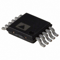
AD5664RBRMZ-3 Analog Devices Inc, AD5664RBRMZ-3 Datasheet - Page 21

AD5664RBRMZ-3
Manufacturer Part Number
AD5664RBRMZ-3
Description
IC DAC NANO 16BIT 1.25V 10-MSOP
Manufacturer
Analog Devices Inc
Series
nanoDAC™r
Specifications of AD5664RBRMZ-3
Data Interface
Serial
Settling Time
4µs
Number Of Bits
16
Number Of Converters
4
Voltage Supply Source
Single Supply
Power Dissipation (max)
6.6mW
Operating Temperature
-40°C ~ 105°C
Mounting Type
Surface Mount
Package / Case
10-MSOP, Micro10™, 10-uMAX, 10-uSOP
Resolution (bits)
16bit
Sampling Rate
220kSPS
Input Channel Type
Serial
Supply Current
950µA
Digital Ic Case Style
SOP
No. Of Pins
10
Lead Free Status / RoHS Status
Lead free / RoHS Compliant
For Use With
EVAL-AD5664REBZ - BOARD EVALUATION FOR AD5664R
Lead Free Status / RoHS Status
Lead free / RoHS Compliant, Lead free / RoHS Compliant
Available stocks
Company
Part Number
Manufacturer
Quantity
Price
Part Number:
AD5664RBRMZ-3
Manufacturer:
ADI/亚德诺
Quantity:
20 000
BIPOLAR OPERATION USING THE
AD5624/AD5664
The AD5624/AD5664 have been designed for single-supply
operation, but a bipolar output range is also possible using the
circuit in Figure 40. The circuit gives an output voltage range of
±5 V. Rail-to-rail operation at the amplifier output is achievable
using an
The output voltage for any input code can be calculated as
follows:
where D represents the input code in decimal (0 to 65536).
With V
This is an output voltage range of ±5 V, with 0x0000 corre-
sponding to a −5 V output, and 0xFFFF corresponding to a
+5 V output.
USING AD5624/AD5664 WITH A
GALVANICALLY ISOLATED INTERFACE
In process control applications in industrial environments, it is
often necessary to use a galvanically isolated interface to protect
and isolate the controlling circuitry from any hazardous
common-mode voltages that might occur in the area where the
DAC is functioning. Isocouplers provide isolation in excess of
3 kV. The AD5624/AD5664 use a 3-wire serial logic interface,
so the ADuM130x 3-channel digital isolator provides the
required isolation (see Figure 41). The power supply to the part
also needs to be isolated, which is done by using a transformer.
On the DAC side of the transformer, a 5 V regulator provides
the 5 V supply required for the AD5624/AD5664.
+5V
V
V
O
O
DD
=
=
AD820
Figure 40. Bipolar Operation with the AD5624/AD5664
= 5 V, R1 = R2 = 10 kΩ,
⎛
⎜
⎝
⎡
⎢
⎣
10µF
V
65
10
DD
,
×
536
D
×
or an
⎛
⎜
⎝
⎞
⎟
⎠
0.1µF
65
−
5
D
,
536
OP295
V
V
⎞
⎟
⎠
DD
INTERFACE
R1 = 10kΩ
AD5624/
AD5664
×
SERIAL
3-WIRE
⎛
⎜
⎝
as the output amplifier.
R1
V
R1
+
OUT
R2
⎞
⎟
⎠
−
V
AD820/
OP295
DD
R2 = 10kΩ
+5V
–5V
×
⎛
⎜
⎝
R2
R1
⎞
⎟
⎠
⎤
⎥
⎦
±5V
Rev. 0 | Page 21 of 24
POWER SUPPLY BYPASSING AND GROUNDING
When accuracy is important in a circuit, it is helpful to consider
carefully the power supply and ground return layout on the
board. The printed circuit board containing the AD5624/
AD5664 should have separate analog and digital sections, each
having its own area of the board. If the AD5624/AD5664 is in a
system where other devices require an AGND-to-DGND
connection, the connection should be made at one point only.
This ground point should be as close as possible to the
AD5624/AD5664.
The power supply to the AD5624/AD5664 should be bypassed
with 10 μF and 0.1 μF capacitors. The capacitors should be
located as close as possible to the device, with the 0.1 μF capacitor
ideally right up against the device. The 10 μF capacitor is the
tantalum bead type. It is important that the 0.1 μF capacitor has
low effective series resistance (ESR) and effective series
inductance (ESI), for example, common ceramic types of
capacitors. This 0.1 μF capacitor provides a low impedance path
to ground for high frequencies caused by transient currents due
to internal logic switching.
The power supply line itself should have as large a trace as
possible to provide a low impedance path and to reduce glitch
effects on the supply line. Clocks and other fast switching
digital signals should be shielded from other parts of the board
by digital ground. Avoid crossover of digital and analog signals
if possible. When traces cross on opposite sides of the board,
ensure that they run at right angles to each other to reduce
feedthrough effects through the board. The best board layout
technique is the microstrip technique where the component
side of the board is dedicated to the ground plane only and the
signal traces are placed on the solder side. However, this is not
always possible with a 2-layer board.
DATA
SCLK
Figure 41. AD5624/AD5664 with a Galvanically Isolated Interface
SDI
POWER
V1A
V1B
V1C
ADuM1300
VOA
VOB
VOC
REGULATOR
5V
SCLK
SYNC
DIN
AD5624/
AD5664
AD5624/AD5664
GND
V
DD
V
10µF
OUT
0.1µF


