DAC102S085CIMM/NOPB National Semiconductor, DAC102S085CIMM/NOPB Datasheet - Page 15
DAC102S085CIMM/NOPB
Manufacturer Part Number
DAC102S085CIMM/NOPB
Description
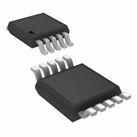
IC DAC 10BIT DUAL 10-MSOP
Manufacturer
National Semiconductor
Series
PowerWise®r
Datasheet
1.DAC102S085CIMMNOPB.pdf
(20 pages)
Specifications of DAC102S085CIMM/NOPB
Settling Time
4.5µs
Number Of Bits
10
Data Interface
Serial
Number Of Converters
2
Voltage Supply Source
Single Supply
Power Dissipation (max)
1.6mW
Operating Temperature
-40°C ~ 105°C
Mounting Type
Surface Mount
Package / Case
10-MSOP, Micro10™, 10-uMAX, 10-uSOP
Number Of Channels
2
Resolution
10b
Interface Type
SER 3W SPI QSPI UW
Single Supply Voltage (typ)
3.3/5V
Dual Supply Voltage (typ)
Not RequiredV
Architecture
Resistor-String
Power Supply Requirement
Single
Output Type
Voltage
Single Supply Voltage (min)
2.7V
Single Supply Voltage (max)
5.5V
Dual Supply Voltage (min)
Not RequiredV
Dual Supply Voltage (max)
Not RequiredV
Operating Temp Range
-40C to 105C
Operating Temperature Classification
Industrial
Mounting
Surface Mount
Pin Count
10
For Use With
DAC102S085EB - BOARD EVALUATION DAC102S085
Lead Free Status / RoHS Status
Lead free / RoHS Compliant
Other names
DAC102S085CIMM
DAC102S085CIMMTR
DAC102S085CIMMTR
Available stocks
Company
Part Number
Manufacturer
Quantity
Price

Part Number:
DAC102S085CIMM/NOPB
Manufacturer:
TI/德州仪器
Quantity:
20 000


Normally, the SYNC line is kept low for at least 16 falling
edges of SCLK and the DAC is updated on the 16th SCLK
falling edge. However, if SYNC is brought high before the 16th
falling edge, the data transfer to the shift register is aborted
and the write sequence is invalid. Under this condition, the
DAC register is not updated and there is no change in the
mode of operation or in the DAC output voltages.
1.6 POWER-ON RESET
The power-on reset circuit controls the output voltages of both
DACs during power-up. Upon application of power, the DAC
registers are filled with zeros and the output voltages are 0V.
The outputs remain at 0V until a valid write sequence is made
to the DAC.
1.7 POWER-DOWN MODES
The DAC102S085 has four power-down modes, two of which
are identical. In power-down mode, the supply current drops
to 20 µA at 3V and 30 µA at 5V. The DAC102S085 is set in
power-down mode by setting OP1 and OP0 to 11. Since this
mode powers down both DACs, the first two bits of the shift
register are used to select different output terminations for the
DAC outputs. Setting A1 and A0 to 00 or 11 causes the out-
puts to be tri-stated (a high impedance state). While setting
A1 and A0 to 01 or 10 causes the outputs to be terminated by
2.5 kΩ or 100 kΩ to ground respectively (see Table 1).
The bias generator, output amplifiers, resistor strings, and
other linear circuitry are all shut down in any of the power-
A1
0
0
1
1
A0
0
1
0
1
TABLE 1. Power-Down Modes
OP1
1
1
1
1
OP0
1
1
1
1
Operating Mode
100 kΩ to GND
High-Z outputs
2.5 kΩ to GND
High-Z outputs
FIGURE 4. Input Register Contents
15
down modes. However, the contents of the DAC registers are
unaffected when in power-down. Each DAC register main-
tains its value prior to the DAC102S085 being powered down
unless it is changed during the write sequence which instruct-
ed it to recover from power down. Minimum power consump-
tion is achieved in the power-down mode with SYNC and
D
(Wake-Up Time) is typically t
Timing Characteristics table.
2.0 Applications Information
2.1 USING REFERENCES AS POWER SUPPLIES
While the simplicity of the DAC102S085 implies ease of use,
it is important to recognize that the path from the reference
input (V
Supply Rejection Ratio (PSRR). Therefore, it is necessary to
provide a noise-free supply voltage to V
lize the full dynamic range of the DAC102S085, the supply
pin (V
same supply voltage. Since the DAC102S085 consumes very
little power, a reference source may be used as the reference
input and/or the supply voltage. The advantages of using a
reference source over a voltage regulator are accuracy and
stability. Some low noise regulators can also be used. Listed
below are a few reference and power supply options for the
DAC102S085.
2.1.1 LM4130
The LM4130, with its 0.05% accuracy over temperature, is a
good choice as a reference source for the DAC102S085. The
4.096V version is useful if a 0 to 4.095V output range is de-
sirable or acceptable. Bypassing the LM4130 VIN pin with a
0.1µF capacitor and the VOUT pin with a 2.2µF capacitor will
improve stability and reduce output noise. The LM4130
comes in a space-saving 5-pin SOT23.
IN
idled low and SCLK disabled. The time to exit power-down
A
) and V
REFIN
) to the VOUTs will have essentially zero Power
REFIN
can be connected together and share the
20195508
WU
µsec as stated in the A.C. and
REFIN
. In order to uti-
www.national.com
Related parts for DAC102S085CIMM/NOPB
Image
Part Number
Description
Manufacturer
Datasheet
Request
R

Part Number:
Description:
National Semiconductor [8-Bit D/A Converter]
Manufacturer:
National Semiconductor
Datasheet:
Part Number:
Description:
National Semiconductor [Media Coprocessor]
Manufacturer:
National Semiconductor
Datasheet:
Part Number:
Description:
Digitally Controlled Tone and Volume Circuit with Stereo Audio Power Amplifier, Microphone Preamp Stage and National 3D Sound
Manufacturer:
National Semiconductor
Datasheet:
Part Number:
Description:
Digitally Controlled Tone and Volume Circuit with Stereo Audio Power Amplifier, Microphone Preamp Stage and National 3D Sound
Manufacturer:
National Semiconductor
Datasheet:
Part Number:
Description:
AC97 Rev 2 Codec with Sample Rate Conversion and National 3D Sound
Manufacturer:
National Semiconductor
Part Number:
Description:
Manufacturer:
National Semiconductor
Datasheet:
Part Number:
Description:
Manufacturer:
National Semiconductor
Datasheet:
Part Number:
Description:
General Purpose, Low Voltage, Low Power, Rail-to-Rail Output Operational Amplifiers
Manufacturer:
National Semiconductor
Datasheet:
Part Number:
Description:
8-bit 20 MSPS flash A/D converter.
Manufacturer:
National Semiconductor
Datasheet:
Part Number:
Description:
Low Noise Quad Operational Amplifier
Manufacturer:
National Semiconductor
Datasheet:
Part Number:
Description:
Quad Differential Line Receivers
Manufacturer:
National Semiconductor
Datasheet:
Part Number:
Description:
Quad High Speed Trapezoidal? Bus Transceiver
Manufacturer:
National Semiconductor
Datasheet:
Part Number:
Description:
Dual Line Receiver
Manufacturer:
National Semiconductor
Datasheet:
Part Number:
Description:
TTL to 10k ECL Level Translator with Latch
Manufacturer:
National Semiconductor
Datasheet: