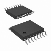
DAC108S085CIMTX/NOPB National Semiconductor, DAC108S085CIMTX/NOPB Datasheet - Page 19

DAC108S085CIMTX/NOPB
Manufacturer Part Number
DAC108S085CIMTX/NOPB
Description
DAC 10BIT MCRPWR OCT R-R 16TSSOP
Manufacturer
National Semiconductor
Series
PowerWise®r
Datasheet
1.DAC108S085CISQNOPB.pdf
(24 pages)
Specifications of DAC108S085CIMTX/NOPB
Settling Time
4.5µs
Number Of Bits
10
Data Interface
Serial
Number Of Converters
8
Voltage Supply Source
Single Supply
Power Dissipation (max)
4.85mW
Operating Temperature
-40°C ~ 125°C
Mounting Type
Surface Mount
Package / Case
16-TSSOP
For Use With
DAC108S085EB - BOARD EVALUATION FOR DAC108S085
Lead Free Status / RoHS Status
Lead free / RoHS Compliant
Other names
DAC108S085CIMTX
Available stocks
Company
Part Number
Manufacturer
Quantity
Price
2.5.2 ADC Reference
shows Channel A of the DAC108S085 providing the drive or
supply voltage for a bridge sensor. By having the sensor sup-
ply voltage adjustable, the output of the sensor can be opti-
mized to the input level of the ADC monitoring it. The output
of the sensor is amplified by a fixed gain amplifier stage with
a differential gain of 1 + 2 × (R
amplifier configuration is the high input impedance seen by
the output of the bridge sensor. The disadvantage is the poor
common-mode rejection ratio (CMRR). The common-mode
voltage (V
output. The V
stage and thus becomes the bias voltage for the input of the
ADC121S705. Channel B of the DAC108S085 is providing
the reference voltage to the ADC121S705. The reference for
the ADC121S705 may be set to any voltage from 1V to 5V,
providing the widest dynamic range possible.
The reference voltage for Channel A and B is powered by an
external 5V power supply. Since the 5V supply is common to
CM
) of the bridge sensor is half of Channel A's DAC
CM
is amplified by a gain of 1V/V by the amplifier
F
/ R
I
). The advantage of this
FIGURE 15. Driving an ADC Reference
FIGURE 14. Industrial Application
19
the sensor supply voltage and the reference voltage of the
ADC, fluctuations in the value of the 5V supply will have a
minimal effect on the digital output code of the ADC. This type
of configuration is often referred to as a "Ratio-metric" design.
For example, an increase of 5% to the 5V supply will cause
the sensor supply voltage to increase by 5%. This causes the
gain or sensitivity of the sensor to increase by 5%. The gain
of the amplifier stage is unaffected by the change in supply
voltage. The ADC121S705 on the other hand, also experi-
ences a 5% increase to its reference voltage. This causes the
size of the ADC's least significant bit (LSB) to increase by 5%.
As a result of the sensor's gain increasing by 5% and the LSB
size of the ADC increasing by the same 5%, there is no net
effect on the circuit's performance. It is assumed that the am-
plifier gain is set low enough to allow for a 5% increase in the
sensor output. Otherwise, the increase in the sensor output
level may cause the output of the amplifiers to clip.
30031256
30031253
www.national.com


