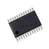
CAT5251YI-00 ON Semiconductor, CAT5251YI-00 Datasheet - Page 7

CAT5251YI-00
Manufacturer Part Number
CAT5251YI-00
Description
Manufacturer
ON Semiconductor
Datasheet
1.CAT5251YI-00.pdf
(15 pages)
Specifications of CAT5251YI-00
Number Of Elements
4
# Of Taps
256
Resistance (max)
100KOhm
Power Supply Requirement
Single
Interface Type
Serial (SPI)
Single Supply Voltage (typ)
3.3/5V
Dual Supply Voltage (typ)
Not RequiredV
Single Supply Voltage (min)
2.5V
Single Supply Voltage (max)
6V
Dual Supply Voltage (min)
Not RequiredV
Dual Supply Voltage (max)
Not RequiredV
Operating Temp Range
-40C to 85C
Operating Temperature Classification
Industrial
Mounting
Surface Mount
Pin Count
24
Package Type
TSSOP
Lead Free Status / Rohs Status
Compliant
Available stocks
Company
Part Number
Manufacturer
Quantity
Price
Part Number:
CAT5251YI-00
Manufacturer:
CSI
Quantity:
20 000
Company:
Part Number:
CAT5251YI-00-T2
Manufacturer:
ON Semiconductor
Quantity:
1 350
INSTRUCTION AND REGISTER
DESCRIPTION
DEVICE TYPE / ADDRESS BYTE
The first byte sent to the CAT5251 from the
master/processor is called the Device Address Byte.
The most significant four bits of the Device Type
address are a device type identifier. These bits for the
CAT5251 are fixed at 0101[B] (refer to Table 1).
The two least significant bits in the slave address
byte, A1 - A0, are the internal slave address and
must match the physical device address which is
defined by the state of the A1 - A0 input pins for the
CAT5251 to successfully continue the command
sequence. Only the device which slave address
matches the incoming device address sent by the
master executes the instruction. The A1 - A0 inputs
can be actively driven by CMOS input signals or tied
to V
address byte must be set to 0.
Table 1. Identification Byte Format
Table 2. Instruction Byte Format
© 2009 SCILLC. All rights reserved.
Characteristics subject to change without notice
CC
or V
SS
. The remaining two bits in the device
(MSB)
(MSB)
ID3
I3
0
ID2
I2
1
Device Type
Identifier
Instruction
Opcode
ID1
I1
0
ID0
I0
1
7
INSTRUCTION BYTE
The next byte sent to the CAT5251 contains the
instruction and register pointer information. The four
most significant bits used provide the instruction
opcode I3-I0. The R1 and R0 bits point to one of the
four data registers of each associated potentiometer.
The least two significant bits point to one of four Wiper
Control Registers. The format is shown in Table 2.
Data Register Selection
R1
0
Data Register Selected
Data Register
Selection
R0
DR0
DR1
DR2
DR3
0
Slave Address
A1
WCR/Pot Selection
P1
R1
0
0
1
1
(LSB)
(LSB)
A0
P0
R0
Doc. No. MD-2017 Rev. H
0
1
0
1
CAT5251


