CAT5251YI-00 ON Semiconductor, CAT5251YI-00 Datasheet - Page 8
CAT5251YI-00
Manufacturer Part Number
CAT5251YI-00
Description
Manufacturer
ON Semiconductor
Datasheet
1.CAT5251YI-00.pdf
(15 pages)
Specifications of CAT5251YI-00
Number Of Elements
4
# Of Taps
256
Resistance (max)
100KOhm
Power Supply Requirement
Single
Interface Type
Serial (SPI)
Single Supply Voltage (typ)
3.3/5V
Dual Supply Voltage (typ)
Not RequiredV
Single Supply Voltage (min)
2.5V
Single Supply Voltage (max)
6V
Dual Supply Voltage (min)
Not RequiredV
Dual Supply Voltage (max)
Not RequiredV
Operating Temp Range
-40C to 85C
Operating Temperature Classification
Industrial
Mounting
Surface Mount
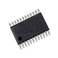
Pin Count
24
Package Type
TSSOP
Lead Free Status / Rohs Status
Compliant
Available stocks
Company
Part Number
Manufacturer
Quantity
Price

Part Number:
CAT5251YI-00
Manufacturer:
CSI
Quantity:
20 000
Company:
Part Number:
CAT5251YI-00-T2
Manufacturer:
ON Semiconductor
Quantity:
1 350


CAT5251
WIPER CONTROL AND DATA REGISTERS
Wiper Control Register (WCR)
The CAT5251 contains four 8-bit Wiper Control
Registers, one for each potentiometer. The Wiper
Control Register output is decoded to select one of
256 switches along its resistor array. The contents of
the WCR can be altered in four ways: it may be
written by the host via Write Wiper Control Register
instruction; it may be written by transferring the
contents of one of four associated Data Registers via
the XFR Data Register instruction; it can be modified
one step at a time by the Increment/decrement
instruction (see Instruction section for more details).
Finally, it is loaded with the content of its data register
zero (DR0) upon power-up.
The Wiper Control Register is a volatile register that
loses its contents when the CAT5251 is powered-
down. Although the register is automatically loaded
with the value in DR0 upon power-up, this may be
different from the value present at power-down.
Data Registers (DR)
Each potentiometer has four 8-bit non-volatile Data
Registers. These can be read or written directly by the
host. Data can also be transferred between any of the
four Data Registers and the associated Wiper Control
Register. Any data changes in one of the Data
Registers is a non-volatile operation and will take a
maximum of 5ms.
Table 3. Instruction Set
Doc. No. MD-2017 Rev. H
Instruction
Read Wiper Control
Register
Write Wiper Control
Register
Read Data Register
Write Data Register
XFR Data Register to
Wiper Control Register
XFR Wiper Control
Register to Data Register
Global XFR Data Registers
to Wiper Control Registers
Global XFR Wiper Control
Registers to Data Register
Increment/Decrement
Wiper Control Register
Read Status (WIP bit)
I3
1
1
1
1
1
1
0
1
0
0
I2
0
0
0
1
1
1
0
0
0
1
I1
0
1
1
0
0
1
0
0
1
0
Instruction Set
I0
1 1/0 1/0
0 1/0 1/0
1
0
1 1/0 1/0
0 1/0 1/0
1 1/0 1/0
0 1/0 1/0
0
1
R1
0
0
0
0
R0
0
0
0
0
WCR1/
1/0
1/0
1/0
1/0
1/0
1/0
1/0
8
P1
0
0
0
If the application does not require storage of multiple
settings for the potentiometer; the Data Registers can
be used as standard memory locations for system
parameters or user preference data.
Write in Process
The contents of the Data Registers are saved to
nonvolatile memory when the CS
after a write sequence is received. The status of the
internal write cycle can be monitored by issuing a
Read Status command to read the Write in Process
(WIP) bit.
INSTRUCTIONS
Four of the ten instructions are three bytes in length.
These instructions are:
— Read Wiper Control Register – read the current
— Write Wiper Control Register – change current
— Read Data Register – read the contents of the
— Write Data Register – write a new value to the
— Read Status – Read the status of the WIP bit which
WCR0/
wiper position of the selected potentiometer in
the WCR
wiper position in the WCR of the selected
potentiometer
selected Data Register
selected Data Register
when set to "1" signifies a write cycle is in progress.
1/0
1/0
1/0
1/0
1/0
1/0
1/0
P0
0
0
1
Operations
Read the contents of the Wiper Control Register
pointed to by P1-P0
Write new value to the Wiper Control Register pointed
to by P1-P0
Read the contents of the Data Register pointed to by
P1-P0 and R1-R0
Write new value to the Data Register pointed to by
P1-P0 and R1-R0
Transfer the contents of the Data Register pointed to
by P1-P0 and R1-R0 to its associated Wiper Control
Register
Transfer the contents of the Wiper Control Register
pointed to by P1-P0 to the Data Register pointed to by
R1-R0
Transfer the contents of the Data Registers pointed to by
R1-R0 of all four pots to their respective Wiper Control
Registers
Transfer the contents of both Wiper Control Registers
to their respective data Registers pointed to by R1-R0
of all four pots
Enable Increment/decrement of the Control Latch
pointed to by P1-P0
Read WIP bit to check internal write cycle status
Characteristics subject to change without notice
Note: 1/0 = data is one or zero
¯¯¯ input goes HIGH
© 2009 SCILLC. All rights reserved.
Related parts for CAT5251YI-00
Image
Part Number
Description
Manufacturer
Datasheet
Request
R

Part Number:
Description:
ON Semiconductor [VOLTAGE REGULATOR]
Manufacturer:
ON Semiconductor
Datasheet:
Part Number:
Description:
357-036-542-201 CARDEDGE 36POS DL .156 BLK LOPRO
Manufacturer:
ON Semiconductor
Datasheet:
Part Number:
Description:
357-036-542-201 CARDEDGE 36POS DL .156 BLK LOPRO
Manufacturer:
ON Semiconductor
Datasheet:
Part Number:
Description:
357-036-542-201 CARDEDGE 36POS DL .156 BLK LOPRO
Manufacturer:
ON Semiconductor
Datasheet:
Part Number:
Description:
357-036-542-201 CARDEDGE 36POS DL .156 BLK LOPRO
Manufacturer:
ON Semiconductor
Datasheet:
Part Number:
Description:
357-036-542-201 CARDEDGE 36POS DL .156 BLK LOPRO
Manufacturer:
ON Semiconductor
Datasheet:
Part Number:
Description:
357-036-542-201 CARDEDGE 36POS DL .156 BLK LOPRO
Manufacturer:
ON Semiconductor
Datasheet:
Part Number:
Description:
357-036-542-201 CARDEDGE 36POS DL .156 BLK LOPRO
Manufacturer:
ON Semiconductor
Datasheet:
Part Number:
Description:
357-036-542-201 CARDEDGE 36POS DL .156 BLK LOPRO
Manufacturer:
ON Semiconductor
Datasheet:
Part Number:
Description:
357-036-542-201 CARDEDGE 36POS DL .156 BLK LOPRO
Manufacturer:
ON Semiconductor
Datasheet:
Part Number:
Description:
357-036-542-201 CARDEDGE 36POS DL .156 BLK LOPRO
Manufacturer:
ON Semiconductor
Datasheet:
Part Number:
Description:
Manufacturer:
ON Semiconductor
Datasheet:
Part Number:
Description:
Manufacturer:
ON Semiconductor
Datasheet:
Part Number:
Description:
Manufacturer:
ON Semiconductor
Datasheet: