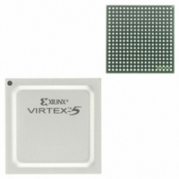
XC2C512-7FGG324C Xilinx Inc, XC2C512-7FGG324C Datasheet - Page 3

XC2C512-7FGG324C
Manufacturer Part Number
XC2C512-7FGG324C
Description
IC CR-II CPLD 512MCELL 324-FBGA
Manufacturer
Xilinx Inc
Series
CoolRunner IIr
Specifications of XC2C512-7FGG324C
Programmable Type
In System Programmable
Delay Time Tpd(1) Max
7.1ns
Voltage Supply - Internal
1.7 V ~ 1.9 V
Number Of Logic Elements/blocks
32
Number Of Macrocells
512
Number Of Gates
12000
Number Of I /o
270
Operating Temperature
0°C ~ 70°C
Mounting Type
Surface Mount
Package / Case
324-FBGA
Features
Programmable
Voltage
1.8V
Memory Type
CMOS
Lead Free Status / RoHS Status
Lead free / RoHS Compliant
Number Of Logic Elements/cells
-
Available stocks
Company
Part Number
Manufacturer
Quantity
Price
Company:
Part Number:
XC2C512-7FGG324C
Manufacturer:
INTEL
Quantity:
578
Absolute Maximum Ratings
DC Electrical Characteristics
DS096 (v3.2) March 8, 2007
Product Specification
Notes:
1.
2.
3.
Notes:
1.
2.
Recommended Operating Conditions
I
I
I
C
C
C
I
I
CCSB
CCSB
CC
IL
IH
Symbol
JTAG
CLK
IO
(2)
(2)
Symbol
V
Maximum DC undershoot below GND must be limited to either 0.5V or 10 mA, whichever is easiest to achieve. During transitions,
the device pins may undershoot to –2.0v or overshoot to +4.5V, provided this over or undershoot lasts less than 10 ns and with the
forcing current being limited to 200 mA.
Valid over commercial temperature range.
For soldering guidelines and thermal considerations, see the
packages, see XAPP427.
16-bit up/down, Resetable binary counter (one counter per function block) tested at
See Quality and Reliability section of the CoolRunner-II family data sheet.
(1)
Symbol
V
V
V
T
CCAUX
V
V
V
V
JTAG
CCAUX
CCIO
STG
V
CCIO
TS
CC
IN
T
CC
J
(1)
(1)
(3)
(2)
R
Standby current Commercial
Standby current Industrial
Dynamic current
JTAG input capacitance
Global clock input capacitance
I/O capacitance
Input leakage current
I/O High-Z leakage
Supply voltage for internal logic and
input buffers
Supply voltage for output drivers @ 3.3V operation
Supply voltage for output drivers @ 2.5V operation
Supply voltage for output drivers @ 1.8V operation
Supply voltage for output drivers @ 1.5V operation
JTAG programming
Supply voltage relative to ground
Supply voltage for output drivers
JTAG input voltage limits
JTAG input supply voltage
Input voltage relative to ground
Voltage applied to 3-state output
Storage Temperature (ambient)
Junction Temperature
Parameter
(Over Recommended Operating Conditions)
Description
Parameter
(1)
V
V
(1)
V
V
IN
IN
www.xilinx.com
CC
CC
Commercial T
Industrial T
= 0V or V
= 0V or V
Test Conditions
= 1.9V, V
= 1.9V, V
Device Packaging
f = 50 MHz
f = 1 MHz
f = 1 MHz
f = 1 MHz
f = 1 MHz
CCIO
CCIO
A
CCIO
CCIO
= –40°C to +85°C
A
to 3.9V
to 3.9V
= 0°C to +70°C
= 3.6V
= 3.6V
information on the Xilinx website. For Pb free
V
CC
= V
Typical
CCIO
150
50
-
-
-
-
-
-
-
XC2C512 CoolRunner-II CPLD
–65 to +150
–0.5 to 2.0
–0.5 to 4.0
–0.5 to 4.0
–0.5 to 4.0
-0.5 to 4.0
-0.5 to 4.0
= 1.9V.
Min
1.7
1.7
3.0
2.3
1.7
1.4
1.7
Value
+150
Max.
+/–1
+/–1
240
400
55
10
12
10
1
Max
1.9
1.9
3.6
2.7
1.9
1.6
3.6
Units
°C
°C
V
V
V
V
V
V
Units
Units
mA
mA
μA
μA
μA
μA
pF
pF
pF
V
V
V
V
V
V
V
3


