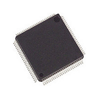
ADSP-2186BST-133R Analog Devices Inc, ADSP-2186BST-133R Datasheet - Page 12

ADSP-2186BST-133R
Manufacturer Part Number
ADSP-2186BST-133R
Description
IC DSP CONTROLLER 16BIT 100LQFP
Manufacturer
Analog Devices Inc
Series
ADSP-21xxr
Type
Fixed Pointr
Datasheet
1.ADSP-2186BSTZ-160.pdf
(36 pages)
Specifications of ADSP-2186BST-133R
Rohs Status
RoHS non-compliant
Interface
Host Interface, Serial Port
Clock Rate
33.3MHz
Non-volatile Memory
External
On-chip Ram
40kB
Voltage - I/o
5.00V
Voltage - Core
5.00V
Operating Temperature
-40°C ~ 85°C
Mounting Type
Surface Mount
Package / Case
100-LQFP
Device Core Size
16b
Format
Fixed Point
Clock Freq (max)
33.3MHz
Mips
33.3
Device Input Clock Speed
33.3MHz
Ram Size
40KB
Operating Supply Voltage (typ)
5V
Operating Supply Voltage (min)
4.5V
Operating Supply Voltage (max)
5.5V
Operating Temp Range
-40C to 85C
Operating Temperature Classification
Industrial
Mounting
Surface Mount
Pin Count
100
Package Type
LQFP
Lead Free Status / Rohs Status
Not Compliant
ADSP-2186
BIASED ROUNDING
A mode is available on the ADSP-2186 to allow biased round-
ing in addition to the normal unbiased rounding. When the
BIASRND bit is set to 0, the normal unbiased rounding opera-
tions occur. When the BIASRND bit is set to 1, biased rounding
occurs instead of the normal unbiased rounding. When operat-
ing in biased rounding mode all rounding operations with MR0
set to 0x8000 will round up, rather than only rounding up odd
MR1 values.
For example:
MR Value
Before RND
00-0000-8000
00-0001-8000
00-0000-8001
00-0001-8001
00-0000-7FFF
00-0001-7FFF
This mode only has an effect when the MR0 register contains
0x8000; all other rounding operations work normally. This
mode allows more efficient implementation of bit-specified
algorithms that use biased rounding, for example the GSM
speech compression routines. Unbiased rounding is preferred
for most algorithms.
Note: BIASRND bit is Bit 12 of the SPORT0 Autobuffer
Control register.
INSTRUCTION SET DESCRIPTION
The ADSP-2186 assembly language instruction set has an alge-
braic syntax that was designed for ease of coding and readability.
The assembly language, which takes full advantage of the
processor’s unique architecture, offers the following benefits:
• The algebraic syntax eliminates the need to remember cryptic
• Every instruction assembles into a single, 24-bit word that
• The syntax is a superset ADSP-2100 Family assembly lan-
• Sixteen condition codes are available. For conditional jump,
• Multifunction instructions allow parallel execution of an
I/O Space Instructions
The instructions used to access the ADSP-2186’s I/O memory
space are as follows:
Syntax: IO(addr) = dreg
assembler mnemonics. For example, a typical arithmetic add
instruction, such as AR = AX0 + AY0, resembles a simple
equation.
can execute in a single instruction cycle.
guage and is completely source and object code compatible
with other family members. Programs may need to be relo-
cated to utilize on-chip memory and conform to the ADSP-
2186’s interrupt vector and reset vector map.
call, return or arithmetic instructions, the condition can be
checked and the operation executed in the same instruction
cycle.
arithmetic instruction with up to two fetches or one write to
processor memory space during a single instruction cycle.
dreg = IO(addr);
Table VII. Biased Rounding Example
Biased
00-0001-8000
00-0002-8000
00-0001-8001
00-0002-8001
00-0000-7FFF
00-0001-7FFF
RND Result
Unbiased
RND Result
00-0000-8000
00-0002-8000
00-0001-8001
00-0002-8001
00-0000-7FFF
00-0001-7FFF
where addr is an address value between 0 and 2047 and dreg is
any of the 16 data registers.
Examples: IO(23) = AR0;
Description: The I/O space read and write instructions move
DESIGNING AN EZ-ICE-COMPATIBLE SYSTEM
The ADSP-2186 has on-chip emulation support and an
ICE-Port, a special set of pins that interface to the EZ-ICE. These
features allow in-circuit emulation without replacing the target
system processor by using only a 14-pin connection from the
target system to the EZ-ICE. Target systems must have a 14-pin
connector to accept the EZ-ICE’s in-circuit probe, a 14-pin plug.
Emulation Reset and the Mode Pins
The Mode A, B, and C pins are located on the rising edge of the
RESET signal. However, when the emulator reset (ERESET) is
asserted by the EZ-ICE, the DSP performs a chip reset, and the
initial mode information is erased, and the logic values on the
mode pins are latched. You must take into consideration the
value of the mode pins before issuing a chip reset command
from the EZ-ICE user interface. If you are using a passive
method of maintaining mode information (as discussed in Set-
ting Memory Modes) then it does not matter that the mode
information is latched by an emulator reset. However, if you are
using the RESET pin as a method of setting the value of the
mode pins, then you have to take into consideration the effects
of an emulator reset.
One method of ensuring that the values located on the mode
pins is the one that is desired to construct a circuit like the one
shown in Figure 9. This circuit will force the value located on
the Mode C pin to zero; regardless if it latched via the RESET
or ERESET pin.
See the ADSP-2100 Family EZ-Tools data sheet for complete
information on ICE products.
The ICE-Port interface consists of the following ADSP-2186
pins:
EBR
EMS
ELIN
EBG
EINT
ELOUT
AR1 = IO(17);
data between the data registers and the I/O
memory space.
1k
ERESET
ECLK
EE
PROGRAMMABLE I/O
ERESET
RESET
MODE A/PFO
ADSP-2186


