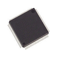
ADSP-2186BST-133R Analog Devices Inc, ADSP-2186BST-133R Datasheet - Page 4

ADSP-2186BST-133R
Manufacturer Part Number
ADSP-2186BST-133R
Description
IC DSP CONTROLLER 16BIT 100LQFP
Manufacturer
Analog Devices Inc
Series
ADSP-21xxr
Type
Fixed Pointr
Datasheet
1.ADSP-2186BSTZ-160.pdf
(36 pages)
Specifications of ADSP-2186BST-133R
Rohs Status
RoHS non-compliant
Interface
Host Interface, Serial Port
Clock Rate
33.3MHz
Non-volatile Memory
External
On-chip Ram
40kB
Voltage - I/o
5.00V
Voltage - Core
5.00V
Operating Temperature
-40°C ~ 85°C
Mounting Type
Surface Mount
Package / Case
100-LQFP
Device Core Size
16b
Format
Fixed Point
Clock Freq (max)
33.3MHz
Mips
33.3
Device Input Clock Speed
33.3MHz
Ram Size
40KB
Operating Supply Voltage (typ)
5V
Operating Supply Voltage (min)
4.5V
Operating Supply Voltage (max)
5.5V
Operating Temp Range
-40C to 85C
Operating Temperature Classification
Industrial
Mounting
Surface Mount
Pin Count
100
Package Type
LQFP
Lead Free Status / Rohs Status
Not Compliant
ADSP-2186
where pin functionality is reconfigurable, the default state is
shown in plain text; alternate functionality is shown in italics.
Common-Mode Pins
Pin
Name(s)
RESET
BR
BG
BGH
DMS
PMS
IOMS
BMS
CMS
RD
WR
IRQ2/
PF7
IRQL0/
PF5
IRQL1/
PF6
IRQE/
PF4
PF3
Mode C/
PF2
Mode B/
PF1
Mode A/
PF0
CLKIN, XTAL 2
CLKOUT
SPORT0
SPORT1
IRQ1:0
FI, FO
PWD
PWDACK
FL0, FL1, FL2 3
V
GND
V
GND
EZ-Port
NOTES
1
2
Interrupt/Flag pins retain both functions concurrently. If IMASK is set to
enable the corresponding interrupts, the DSP will vector to the appropriate
interrupt vector address when the pin is asserted, either by external devices or
set as a programmable flag.
SPORT configuration determined by the DSP System Control Register. Soft-
ware configurable.
DD
DD
#
of
Pins put
1
1
1
1
1
1
1
1
1
1
1
1
1
1
1
1
1
1
1
1
5
5
1
1
6
10
11
20
9
Input/
Out-
I
I
O
O
O
O
O
O
O
O
O
I
I/O
I
I/O
I
I/O
I
I/O
I/O
I
I/O
I
I/O
I
I/O
I
O
I/O
I/O
I
O
O
I
I
I
I
I/O
Function
Processor Reset Input
Bus Request Input
Bus Grant Output
Bus Grant Hung Output
Data Memory Select Output
Program Memory Select Output
Memory Select Output
Byte Memory Select Output
Combined Memory Select Output
Memory Read Enable Output
Memory Write Enable Output
Edge- or Level-Sensitive
Interrupt Request
Programmable I/O Pin
Level-Sensitive Interrupt Requests
Programmable I/O Pin
Level-Sensitive Interrupt Requests
Programmable I/O Pin
Edge-Sensitive Interrupt Requests
Programmable I/O Pin
Programmable I/O Pin
Mode Select Input—Checked
only During RESET
Programmable I/O Pin During
Normal Operation
Mode Select Input—Checked
only During RESET
Programmable I/O Pin During
Normal Operation
Mode Select Input—Checked
only During RESET
Programmable I/O Pin During
Normal Operation
Clock or Quartz Crystal Input
Processor Clock Output
Serial Port I/O Pins
Serial Port I/O Pins
Edge- or Level-Sensitive Interrupts,
Flag In, Flag Out
Power-Down Control Input
Power-Down Control Output
Output Flags
Power (LQFP)
Ground (LQFP)
Power (Mini-BGA)
Ground (Mini-BGA)
For Emulation Use
2
1
1
1
1
Memory Interface Pins
The ADSP-2186 processor can be used in one of two modes:
Full Memory Mode, which allows BDMA operation with full
external overlay memory and I/O capability, or Host Mode,
which allows IDMA operation with limited external addressing
capabilities. The operating mode is determined by the state of
the Mode C pin during RESET and cannot be changed while
the processor is running.
Full Memory Mode Pins (Mode C = 0)
Pin Name
A13:0
D23:0
Host Mode Pins (Mode C = 1)
Pin Name
IAD15:0
A0
D23:8
IWR
IRD
IAL
IS
IACK
In Host Mode, external peripheral addresses can be decoded using the A0,
CMS, PMS, DMS, and IOMS signals.
Terminating Unused Pin
The following table shows the recommendations for terminating
unused pins.
Pin Terminations
Pin
Name
XTAL
CLKOUT
A13:1 or
IAD12:0
A0
D23:8
D7 or
IWR
D6 or
IRD
D5 or
IAL
I/O
3-State
(Z)
I
O
O (Z)
I/O (Z)
O (Z)
I/O (Z)
I/O (Z)
I
I/O (Z)
I
I/O (Z)
I
#
of
Pins
14
24
#
of
Pins
16
1
16
1
1
1
1
1
Input/
Output
O
I/O
Input/
Output
I/O
O
I/O
I
I
I
I
O
Reset
State
I
O
Hi-Z
Hi-Z
Hi-Z
Hi-Z
Hi-Z
I
Hi-Z
I
Hi-Z
I
Hi-Z
Caused
By
BR, EBR
IS
BR, EBR
BR, EBR
BR, EBR
BR, EBR
BR, EBR
gram, Data, Byte and I/O Spaces
Data, Byte and I/O Spaces
(8 MSBs Are Also Used as
Byte Memory Addresses)
Program, Data, or Byte Access
Data Byte and I/O Spaces
Data I/O Pins for Program,
Data I/O Pins for Program,
Function
Address Output Pins for Pro-
Function
IDMA Port Address/Data Bus
Address Pin for External I/O,
IDMA Write Enable
IDMA Read Enable
IDMA Address Latch Pin
IDMA Select
IDMA Port Acknowledge
Unused
Float
Float
High (Inactive)
High (Inactive)
Low (Inactive)
Configuration
Float
Float
Float
Float
Float
Float
Float


