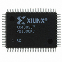
XC4005L-5PQ100C Xilinx Inc, XC4005L-5PQ100C Datasheet - Page 20

XC4005L-5PQ100C
Manufacturer Part Number
XC4005L-5PQ100C
Description
IC 3.3V FPGA 196 CLB'S 100-PQFP
Manufacturer
Xilinx Inc
Series
XC4000r
Datasheet
1.XC4005L-5PC84C.pdf
(175 pages)
Specifications of XC4005L-5PQ100C
Number Of Logic Elements/cells
466
Number Of Labs/clbs
196
Total Ram Bits
6272
Number Of I /o
77
Number Of Gates
5000
Voltage - Supply
3 V ~ 3.6 V
Mounting Type
Surface Mount
Operating Temperature
0°C ~ 85°C
Package / Case
100-BQFP
Lead Free Status / RoHS Status
Contains lead / RoHS non-compliant
Other names
122-1121
Available stocks
Company
Part Number
Manufacturer
Quantity
Price
XC4000 Series Field Programmable Gate Arrays
Input/Output Blocks (IOBs)
User-configurable input/output blocks (IOBs) provide the
interface between external package pins and the internal
logic. Each IOB controls one package pin and can be con-
figured for input, output, or bidirectional signals.
Figure 16
XC4000E IOB. A more complete diagram of the XC4000E
IOB can be found in
Scan” section.
in the IOB.
Figure 17
XC4000EX IOB. The XC4000EX IOB contains some spe-
cial features not included in the XC4000E IOB. These fea-
tures are highlighted in
throughout this section. When XC4000EX special features
are discussed, they are clearly identified in the text. Any
feature not so identified is present in both XC4000E and
XC4000EX devices.
IOB Input Signals
Two paths, labeled I1 and I2 in
bring input signals into the array. Inputs also connect to an
input register that can be programmed as either an edge-
triggered flip-flop or a level-sensitive latch.
The choice is made by placing the appropriate library sym-
bol. For example, IFD is the basic input flip-flop (rising
edge triggered), and ILD is the basic input latch (transpar-
ent-High). Variations with inverted clocks are available, and
some combinations of latches and flip-flops can be imple-
mented in a single IOB, as described in the XACT Libraries
Guide .
The inputs can be globally configured for either TTL (1.2V,
default) or CMOS thresholds, using an option in the Make-
Bits program. There is a slight hysteresis of about 300mV.
The output levels are also configurable; the two global
adjustments of input threshold and output level are inde-
pendent.
Inputs of the low-voltage devices must be configured as
CMOS at all times. They can be driven by the outputs of all
5-Volt XC4000-Series devices, provided that the 5-Volt out-
puts are in TTL mode. They can also be driven by any TTL
output that does not exceed 3.7 V. 5-Volt XC3000-family
device outputs, for example, are TTL-compatible, but since
the output voltage can exceed 3.7 V, they cannot be used to
drive an XC4000L or XC4000XL input.
The inputs of XC4000-Series 5-Volt devices can be driven
by the outputs of any 3.3-Volt device, if the 5-Volt inputs are
in TTL mode.
Supported sources for XC4000-Series device inputs are
shown in
4-24
Table
shows a simplified block diagram of the
shows a simplified block diagram of the
Figure 42
10.
Figure 42 on page
includes the boundary scan logic
Figure
Figure 16
17, and discussed
51, in the “Boundary
and
Figure
17,
Table 10: Supported Sources for XC4000-Series Device
Inputs
Registered Inputs
The I1 and I2 signals that exit the block can each carry
either the direct or registered input signal.
The input and output storage elements in each IOB have a
common clock enable input, which, through configuration,
can be activated individually for the input or output flip-flop,
or both. This clock enable operates exactly like the EC pin
on the XC4000-Series CLB. It cannot be inverted within
the IOB.
The storage element behavior is shown in
Table 11: Input Register Functionality
(active rising edge is shown)
Any device, Vcc = 3.3 V,
CMOS outputs
XC4000-Series, Vcc = 5 V,
TTL outputs
Any device, Vcc = 5 V,
TTL outputs (Voh
Any device, Vcc = 5 V,
CMOS outputs
Power-Up or
GSR
Flip-Flop
Latch
Both
Legend:
Mode
__/
SR
0*
1*
X
1. Acceptable for XC4000XL if the designated 5-Volt
supply pad (V
Source
Don’t care
Rising edge
Set or Reset value. Reset is default.
Input is Low or unconnected (default value)
Input is High or unconnected (default value)
Clock
__/
X
X
0
3.7 V)
1
0
TT
September 18, 1996 (Version 1.04)
) is tied to 5V.
Danger
CMOS
Enable
3.3 V,
Clock
XC4000-Series Inputs
1*
1*
1*
X
X
0
1
TTL
5 V,
Table
D
X
D
X
X
D
X
11.
Unreli-
CMOS
Data
able
5 V,
SR
Q
D
Q
Q
D
Q


