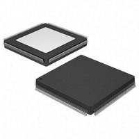
XA3S50-4PQG208I Xilinx Inc, XA3S50-4PQG208I Datasheet - Page 2

XA3S50-4PQG208I
Manufacturer Part Number
XA3S50-4PQG208I
Description
IC FPGA SPARTAN-3 50K 208-PQFP
Manufacturer
Xilinx Inc
Series
Spartan™-3 XAr
Datasheet
1.XA3S50-4VQG100I.pdf
(8 pages)
Specifications of XA3S50-4PQG208I
Number Of Logic Elements/cells
1728
Number Of Labs/clbs
192
Total Ram Bits
73728
Number Of I /o
124
Number Of Gates
50000
Voltage - Supply
1.14 V ~ 1.26 V
Mounting Type
Surface Mount
Operating Temperature
-40°C ~ 100°C
Package / Case
208-BFQFP
Lead Free Status / RoHS Status
Lead free / RoHS Compliant
Available stocks
Company
Part Number
Manufacturer
Quantity
Price
•
•
•
•
•
•
Please refer to the Spartan-3 complete data sheet (DS099)
for a full product description, AC and DC specifications, and
package pinout descriptions
Architectural Overview
The Spartan-3 family architecture consists of five
fundamental programmable functional elements:
•
DS314 (v1.3) June 18, 2009
Product Specification
♦
♦
♦
SelectRAM™ hierarchical memory
♦
♦
Digital Clock Manager (up to four DCMs)
♦
♦
♦
♦
Fully supported by Xilinx ISE® software development
system
♦
MicroBlaze™ processor, CAN, LIN, MOST, and other
cores
Pb-free packaging options
Xilinx and all of our production partners are qualified to
ISO-TS16949
Configurable Logic Blocks (CLBs) contain RAM-based
Look-Up Tables (LUTs) to implement logic and storage
Fast look-ahead carry logic
Dedicated 18 x 18 multipliers
JTAG logic compatible with IEEE 1149.1/1532
Up to 576 Kbits of total block RAM
Up to 208 Kbits of total distributed RAM
Clock skew elimination
Frequency synthesis
High-resolution phase shifting
Maximum clock frequency 125 MHz
Synthesis, mapping, placement and routing
R
www.xilinx.com
•
•
•
•
These elements are organized as shown in
of IOBs surrounds a regular array of CLBs. The XA3S50
has a single column of block RAM embedded in the array.
Those devices ranging from the XA3S200 to the XA3S1500
have two columns of block RAM. Each column is made up
of several 18 Kbit RAM blocks; each block is associated
with a dedicated multiplier. The DCMs are positioned at the
ends of the block RAM columns.
The Spartan-3 family features a rich network of traces and
switches that interconnect all five functional elements,
transmitting signals among them. Each functional element
has an associated switch matrix that permits multiple
connections to the routing.
elements that can be used as flip-flops or latches.
CLBs can be programmed to perform a wide variety of
logical functions as well as to store data.
Input/Output Blocks (IOBs) control the flow of data
between the I/O pins and the internal logic of the
device. Each IOB supports bidirectional data flow plus
3-state operation. Twenty-six different signal standards,
including eight high-performance differential standards,
are available as shown in
(DDR) registers are included. The Digitally Controlled
Impedance (DCI) feature provides automatic on-chip
terminations, simplifying board designs.
Block RAM provides data storage in the form of 18-Kbit
dual-port blocks.
Multiplier blocks accept two 18-bit binary numbers as
inputs and calculate the product.
Digital Clock Manager (DCM) blocks provide
self-calibrating, fully digital solutions for distributing,
delaying, multiplying, dividing, and phase shifting clock
signals.
Introduction and Ordering Information
Table
2. Double Data-Rate
Figure
1. A ring
2


