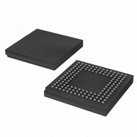
XC3S250E-5CPG132C Xilinx Inc, XC3S250E-5CPG132C Datasheet - Page 13

XC3S250E-5CPG132C
Manufacturer Part Number
XC3S250E-5CPG132C
Description
IC FPGA SPARTAN-3E 250K 132CSBGA
Manufacturer
Xilinx Inc
Series
Spartan™-3Er
Datasheet
1.XC3S100E-4VQG100C.pdf
(233 pages)
Specifications of XC3S250E-5CPG132C
Number Of Logic Elements/cells
5508
Number Of Labs/clbs
612
Total Ram Bits
221184
Number Of I /o
92
Number Of Gates
250000
Voltage - Supply
1.14 V ~ 1.26 V
Mounting Type
Surface Mount
Operating Temperature
0°C ~ 85°C
Package / Case
132-TFBGA, CSPBGA
Lead Free Status / RoHS Status
Lead free / RoHS Compliant
Available stocks
Company
Part Number
Manufacturer
Quantity
Price
Company:
Part Number:
XC3S250E-5CPG132C
Manufacturer:
Xilinx Inc
Quantity:
10 000
- Current page: 13 of 233
- Download datasheet (6Mb)
Storage Element Functions
There are three pairs of storage elements in each IOB, one
pair for each of the three paths. It is possible to configure
each of these storage elements as an edge-triggered
D-type flip-flop (FD) or a level-sensitive latch (LD).
The storage-element pair on either the Output path or the
Three-State path can be used together with a special multi-
plexer to produce Double-Data-Rate (DDR) transmission.
Table 4: Storage Element Signal Description
As shown in
and three-state paths share a common clock. The OTCLK1
clock signal drives the CK clock inputs of the upper registers
on the output and three-state paths. Similarly, OTCLK2
drives the CK inputs for the lower registers on the output
and three-state paths. The upper and lower registers on the
input path have independent clock lines: ICLK1 and ICLK2.
The OCE enable line controls the CE inputs of the upper
and lower registers on the output path. Similarly, TCE con-
Table 5: Storage Element Options
DS312-2 (v3.8) August 26, 2009
Product Specification
D
Q
CK
CE
SR
REV
FF/Latch
SYNC/ASYNC
Element
Storage
Signal
Option Switch
R
Data input
Data output
Clock input
Clock Enable input
Set/Reset input
Reverse input
Figure
Description
5, the upper registers in both the output
Chooses between an edge-triggered flip-flop
or a level-sensitive latch
Determines whether the SR set/reset control is
synchronous or asynchronous
When asserted, this input enables CK. If not connected, CE defaults to the asserted
Data at this input is stored on the active edge of CK and enabled by CE. For latch
operation when the input is enabled, data passes directly to the output Q.
The data on this output reflects the state of the storage element. For operation as a latch
in transparent mode, Q mirrors the data at D.
Data is loaded into the storage element on this input’s active edge with CE asserted.
state.
This input forces the storage element into the state specified by the SRHIGH/SRLOW
attributes. The SYNC/ASYNC attribute setting determines if the SR input is
synchronized to the clock or not. If both SR and REV are active at the same time, the
storage element gets a value of 0.
This input is used together with SR. It forces the storage element into the state opposite
from what SR does. The SYNC/ASYNC attribute setting determines whether the REV
input is synchronized to the clock or not. If both SR and REV are active at the same time,
the storage element gets a value of 0.
Function
www.xilinx.com
This is accomplished by taking data synchronized to the
clock signal’s rising edge and converting it to bits syn-
chronized on both the rising and the falling edge. The com-
bination of two registers and a multiplexer is referred to as a
Double-Data-Rate D-type flip-flop (ODDR2).
Table 4
age element.
trols the CE inputs for the register pair on the three-state
path and ICE does the same for the register pair on the
input path.
The Set/Reset (SR) line entering the IOB controls all six
registers, as is the Reverse (REV) line.
In addition to the signal polarity controls described in
Overview, each storage element additionally supports the
controls described in
Independent for each storage element
Independent for each storage element
describes the signal paths associated with the stor-
Function
Table
Specificity
5.
Functional Description
IOB
13
Related parts for XC3S250E-5CPG132C
Image
Part Number
Description
Manufacturer
Datasheet
Request
R

Part Number:
Description:
IC SPARTAN-3E FPGA 250K 144TQFP
Manufacturer:
Xilinx Inc
Datasheet:

Part Number:
Description:
IC SPARTAN-3E FPGA 250K 256-FTBG
Manufacturer:
Xilinx Inc
Datasheet:

Part Number:
Description:
IC FPGA SPARTAN-3E 250K 256-FTBG
Manufacturer:
Xilinx Inc
Datasheet:

Part Number:
Description:
IC FPGA SPARTAN 3E 144TQFP
Manufacturer:
Xilinx Inc
Datasheet:

Part Number:
Description:
FPGA Spartan®-3E Family 250K Gates 5508 Cells 572MHz 90nm (CMOS) Technology 1.2V 256-Pin FTBGA
Manufacturer:
Xilinx Inc
Datasheet:

Part Number:
Description:
FPGA Spartan®-3E Family 250K Gates 5508 Cells 572MHz 90nm (CMOS) Technology 1.2V 208-Pin PQFP
Manufacturer:
Xilinx Inc
Datasheet:

Part Number:
Description:
FPGA Spartan®-3E Family 250K Gates 5508 Cells 572MHz 90nm (CMOS) Technology 1.2V 208-Pin PQFP
Manufacturer:
Xilinx Inc
Datasheet:

Part Number:
Description:
FPGA Spartan®-3E Family 250K Gates 5508 Cells 572MHz 90nm (CMOS) Technology 1.2V 144-Pin TQFP
Manufacturer:
Xilinx Inc
Datasheet:

Part Number:
Description:
FPGA Spartan®-3E Family 250K Gates 5508 Cells 572MHz 90nm (CMOS) Technology 1.2V 256-Pin FTBGA
Manufacturer:
Xilinx Inc
Datasheet:

Part Number:
Description:
FPGA Spartan®-3E Family 250K Gates 5508 Cells 572MHz 90nm (CMOS) Technology 1.2V 100-Pin VTQFP
Manufacturer:
Xilinx Inc
Datasheet:

Part Number:
Description:
FPGA Spartan®-3E Family 250K Gates 5508 Cells 572MHz 90nm (CMOS) Technology 1.2V 144-Pin TQFP
Manufacturer:
Xilinx Inc
Datasheet:

Part Number:
Description:
IC FPGA SPARTAN-3E 250K 100-VQFP
Manufacturer:
Xilinx Inc
Datasheet:

Part Number:
Description:
IC FPGA SPARTAN-3E 250K 132CSBGA
Manufacturer:
Xilinx Inc
Datasheet:

Part Number:
Description:
IC FPGA SPARTAN-3E 250K 144-TQFP
Manufacturer:
Xilinx Inc
Datasheet:

Part Number:
Description:
IC FPGA SPARTAN-3E 250K 208-PQFP
Manufacturer:
Xilinx Inc
Datasheet:


