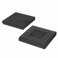
XC3S250E-5CPG132C Xilinx Inc, XC3S250E-5CPG132C Datasheet - Page 80

XC3S250E-5CPG132C
Manufacturer Part Number
XC3S250E-5CPG132C
Description
IC FPGA SPARTAN-3E 250K 132CSBGA
Manufacturer
Xilinx Inc
Series
Spartan™-3Er
Datasheet
1.XC3S100E-4VQG100C.pdf
(233 pages)
Specifications of XC3S250E-5CPG132C
Number Of Logic Elements/cells
5508
Number Of Labs/clbs
612
Total Ram Bits
221184
Number Of I /o
92
Number Of Gates
250000
Voltage - Supply
1.14 V ~ 1.26 V
Mounting Type
Surface Mount
Operating Temperature
0°C ~ 85°C
Package / Case
132-TFBGA, CSPBGA
Lead Free Status / RoHS Status
Lead free / RoHS Compliant
Available stocks
Company
Part Number
Manufacturer
Quantity
Price
Company:
Part Number:
XC3S250E-5CPG132C
Manufacturer:
Xilinx Inc
Quantity:
10 000
- Current page: 80 of 233
- Download datasheet (6Mb)
Functional Description
Table 55: Serial Peripheral Interface (SPI) Connections
80
HSWAP
M[2:0]
VS[2:0]
MOSI
DIN
CSO_B
CCLK
DOUT
INIT_B
Pin Name
P
S
bidirectional
Open-drain
Direction
Output
Output
Output
Output
FPGA
Input
Input
Input
Input
I/O
User I/O Pull-Up Control. When Low
during configuration, enables pull-up
resistors in all I/O pins to respective I/O
bank V
0: Pull-ups during configuration
1: No pull-ups
Mode Select. Selects the FPGA
configuration mode. See
Considerations for the HSWAP,
M[2:0], and VS[2:0]
Variant Select. Instructs the FPGA how
to communicate with the attached SPI
Flash PROM. See
Considerations for the HSWAP,
M[2:0], and VS[2:0]
Serial Data Output.
Serial Data Input.
Chip Select Output. Active Low.
Configuration Clock. Generated by
FPGA internal oscillator. Frequency
controlled by ConfigRate bitstream
generator option. If CCLK PCB trace is
long or has multiple connections,
terminate this output to maintain signal
integrity. See
Considerations.
Serial Data Output.
Initialization Indicator. Active Low.
Goes Low at start of configuration during
Initialization memory clearing process.
Released at end of memory clearing,
when mode select pins are sampled. In
daisy-chain applications, this signal
requires an external 4.7 kΩ pull-up
resistor to VCCO_2.
CCO
input.
CCLK Design
Description
Design
Pins.
Pins.
Design
www.xilinx.com
Drive at valid logic level
throughout configuration.
M2 = 0, M1 = 0, M0 = 1.
Sampled when INIT_B goes
High.
Must be at the logic levels
shown in
when INIT_B goes High.
FPGA sends SPI Flash memory
read commands and starting
address to the PROM’s serial
data input.
FPGA receives serial data from
PROM’s serial data output.
Connects to the SPI Flash
PROM’s chip-select input. If
HSWAP = 1, connect this signal
to a 4.7 kΩ pull-up resistor to
3.3V.
Drives PROM’s clock input.
Actively drives. Not used in
single-FPGA designs. In a
daisy-chain configuration, this
pin connects to DIN input of the
next FPGA in the chain.
Active during configuration. If
SPI Flash PROM requires > 2
ms to awake after powering on,
hold INIT_B Low until PROM is
ready. If CRC error detected
during configuration, FPGA
drives INIT_B Low.
During Configuration
Table
53. Sampled
DS312-2 (v3.8) August 26, 2009
User I/O
User I/O
User I/O
User I/O
User I/O
Drive CSO_B High after
configuration to disable the
SPI Flash and reclaim the
MOSI, DIN, and CCLK pins.
Optionally, re-use this pin
and MOSI, DIN, and CCLK
to continue communicating
with SPI Flash.
User I/O
User I/O
User I/O. If unused in the
application, drive INIT_B
High.
After Configuration
Product Specification
R
Related parts for XC3S250E-5CPG132C
Image
Part Number
Description
Manufacturer
Datasheet
Request
R

Part Number:
Description:
IC SPARTAN-3E FPGA 250K 144TQFP
Manufacturer:
Xilinx Inc
Datasheet:

Part Number:
Description:
IC SPARTAN-3E FPGA 250K 256-FTBG
Manufacturer:
Xilinx Inc
Datasheet:

Part Number:
Description:
IC FPGA SPARTAN-3E 250K 256-FTBG
Manufacturer:
Xilinx Inc
Datasheet:

Part Number:
Description:
IC FPGA SPARTAN 3E 144TQFP
Manufacturer:
Xilinx Inc
Datasheet:

Part Number:
Description:
FPGA Spartan®-3E Family 250K Gates 5508 Cells 572MHz 90nm (CMOS) Technology 1.2V 256-Pin FTBGA
Manufacturer:
Xilinx Inc
Datasheet:

Part Number:
Description:
FPGA Spartan®-3E Family 250K Gates 5508 Cells 572MHz 90nm (CMOS) Technology 1.2V 208-Pin PQFP
Manufacturer:
Xilinx Inc
Datasheet:

Part Number:
Description:
FPGA Spartan®-3E Family 250K Gates 5508 Cells 572MHz 90nm (CMOS) Technology 1.2V 208-Pin PQFP
Manufacturer:
Xilinx Inc
Datasheet:

Part Number:
Description:
FPGA Spartan®-3E Family 250K Gates 5508 Cells 572MHz 90nm (CMOS) Technology 1.2V 144-Pin TQFP
Manufacturer:
Xilinx Inc
Datasheet:

Part Number:
Description:
FPGA Spartan®-3E Family 250K Gates 5508 Cells 572MHz 90nm (CMOS) Technology 1.2V 256-Pin FTBGA
Manufacturer:
Xilinx Inc
Datasheet:

Part Number:
Description:
FPGA Spartan®-3E Family 250K Gates 5508 Cells 572MHz 90nm (CMOS) Technology 1.2V 100-Pin VTQFP
Manufacturer:
Xilinx Inc
Datasheet:

Part Number:
Description:
FPGA Spartan®-3E Family 250K Gates 5508 Cells 572MHz 90nm (CMOS) Technology 1.2V 144-Pin TQFP
Manufacturer:
Xilinx Inc
Datasheet:

Part Number:
Description:
IC FPGA SPARTAN-3E 250K 100-VQFP
Manufacturer:
Xilinx Inc
Datasheet:

Part Number:
Description:
IC FPGA SPARTAN-3E 250K 132CSBGA
Manufacturer:
Xilinx Inc
Datasheet:

Part Number:
Description:
IC FPGA SPARTAN-3E 250K 144-TQFP
Manufacturer:
Xilinx Inc
Datasheet:

Part Number:
Description:
IC FPGA SPARTAN-3E 250K 208-PQFP
Manufacturer:
Xilinx Inc
Datasheet:


