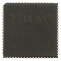
XC3020A-7PC68C Xilinx Inc, XC3020A-7PC68C Datasheet - Page 29

XC3020A-7PC68C
Manufacturer Part Number
XC3020A-7PC68C
Description
IC LOGIC CL ARRAY 2000GAT 68PLCC
Manufacturer
Xilinx Inc
Series
XC3000A/Lr
Datasheet
1.XC3190A-3PC84C.pdf
(76 pages)
Specifications of XC3020A-7PC68C
Number Of Labs/clbs
64
Total Ram Bits
14779
Number Of I /o
58
Number Of Gates
1500
Voltage - Supply
4.75 V ~ 5.25 V
Mounting Type
Surface Mount
Operating Temperature
0°C ~ 85°C
Package / Case
68-LCC (J-Lead)
Lead Free Status / RoHS Status
Contains lead / RoHS non-compliant
Number Of Logic Elements/cells
-
Other names
122-1009
Available stocks
Company
Part Number
Manufacturer
Quantity
Price
Part Number:
XC3020A-7PC68C
Manufacturer:
XILINX/赛灵思
Quantity:
20 000
Slave Serial Mode
In Slave Serial mode, an external signal drives the CCLK
input(s) of the FPGA(s). The serial configuration bitstream
must be available at the DIN input of the lead FPGA a short
set-up time before each rising CCLK edge. The lead device
then presents the preamble data (and all data that over-
Figure 29: Slave Serial Mode Circuit Diagram
November 9, 1998 (Version 3.1)
R
RESET
Product Obsolete or Under Obsolescence
Computer
Micro
Port
I/O
STRB
D0
D1
D2
D3
D4
D5
D6
D7
+5 V
+5 V
XC3000 Series Field Programmable Gate Arrays
CCLK
DIN
INIT
RESET
M0
flows the lead device) on its DOUT pin. There is an internal
delay of 0.5 CCLK periods, which means that DOUT
changes on the falling CCLK edge, and the next device in
the daisy-chain accepts data on the subsequent rising
CCLK edge.
D/P
*
M1
FPGA
PWRDWN
I/O Pins
Other
DOUT
HDC
LDC
M2
5 k
General-
Purpose
User I/O
Pins
*
Optional
Daisy-Chained
LCAs with
Different
Configurations
Activated, a
5-k Resistor is
Required in
Series with M1
If Readback is
X5993
7-31
7


