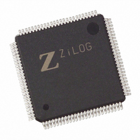
EZ80190AZ050SG Zilog, EZ80190AZ050SG Datasheet - Page 152

EZ80190AZ050SG
Manufacturer Part Number
EZ80190AZ050SG
Description
IC WEBSERVER 8 BIT 50MHZ 100LQFP
Manufacturer
Zilog
Datasheet
1.EZ80190AZ050SG.pdf
(221 pages)
Specifications of EZ80190AZ050SG
Processor Type
eZ80
Features
High Speed, Single-Cycle Instruction-Fetch
Speed
50MHz
Voltage
3.3V
Mounting Type
Surface Mount
Package / Case
100-LQFP
Processor Series
EZ80190x
Core
eZ80
Data Bus Width
8 bit
Program Memory Type
ROMLess
Data Ram Size
8 KB
Interface Type
I2C, IrDA, SPI, UART
Maximum Clock Frequency
50 MHz
Number Of Programmable I/os
32
Number Of Timers
6
Operating Supply Voltage
3 V to 3.6 V
Maximum Operating Temperature
+ 105 C
Mounting Style
SMD/SMT
Minimum Operating Temperature
- 40 C
Lead Free Status / RoHS Status
Lead free / RoHS Compliant
Other names
269-3866
EZ80190AZ050SG
EZ80190AZ050SG
Available stocks
Company
Part Number
Manufacturer
Quantity
Price
Company:
Part Number:
EZ80190AZ050SG
Manufacturer:
ZiLOG
Quantity:
135
- Current page: 152 of 221
- Download datasheet (4Mb)
DMA Channel Priorities
DMA Interrupts
DMA Control Registers
Table 76. DMA Registers
PS006614-1208
Name
DMA0_SAR_L
DMA0_SAR_H
DMA0_SAR_U
In all operating mode combinations, DMA Channel 0 is prioritized higher than DMA
Channel 1. If Channel 0 is configured for BURST mode operation, Channel 0 completes
its entire block transfer before Channel 1 begins its transfer.
When both channels are configured for CYCLE-STEAL mode, the 2 DMA channels alter-
nate stealing execution cycles from the CPU. First, DMA Channel 0 performs a cycle-steal
single-byte transfer then releases the bus to the CPU for the next 8 clock cycles. Then,
DMA channel 1 requests the bus and gains access to pass one of its bytes. After DMA
channel 1 completes the transfer of its byte, control is returned to the CPU for another
8 clock cycles. This process repeats until one or both of the DMA channels complete the
transfer of all required bytes.
If DMA channel 0 is programmed in CYCLE-STEAL mode and DMA channel 1 is pro-
grammed in BURST mode, DMA channel 1 is not allowed to transfer its data until DMA
channel 0 completes its entire transfer.
Each DMA controller can generate an interrupt request to the CPU when its memory
transfer is complete. The DMA interrupts are enabled by setting bit 6 in the DMA Control
register (either DMA0_CTL or DMA1_CTL) to 1. The default operation is for the DMA
interrupts to be disabled. Each DMA channel is capable of generating an interrupt when its
16-bit data byte transfer counter register reaches its terminal count of
rupts are cleared by resetting the DMA_EN bit field in the DMA Control registers to dis-
able the DMA channel that is generating the input. Clearing the interrupt enable bit
(DMAx_CTL[6] = IRQ_DMA) does not clear the interrupt to the CPU after it is set.
Table 76
accessed by the CPU using I/O instructions.
Description
DMA0 Source Address Low Byte register
DMA0 Source Address High Byte register
DMA0 Source Address Upper Byte register
lists the control registers used by the DMA controller. These registers are
Access
CPU
R/W
R/W
R/W
Direct Memory Access Controller
Product Specification
Reset
Value
0000h
XX
XX
XX
. The inter-
Register
Address
eZ80190
EEh
EFh
F0h
142
Related parts for EZ80190AZ050SG
Image
Part Number
Description
Manufacturer
Datasheet
Request
R

Part Number:
Description:
Communication Controllers, ZILOG INTELLIGENT PERIPHERAL CONTROLLER (ZIP)
Manufacturer:
Zilog, Inc.
Datasheet:

Part Number:
Description:
KIT DEV FOR Z8 ENCORE 16K TO 64K
Manufacturer:
Zilog
Datasheet:

Part Number:
Description:
KIT DEV Z8 ENCORE XP 28-PIN
Manufacturer:
Zilog
Datasheet:

Part Number:
Description:
DEV KIT FOR Z8 ENCORE 8K/4K
Manufacturer:
Zilog
Datasheet:

Part Number:
Description:
KIT DEV Z8 ENCORE XP 28-PIN
Manufacturer:
Zilog
Datasheet:

Part Number:
Description:
DEV KIT FOR Z8 ENCORE 4K TO 8K
Manufacturer:
Zilog
Datasheet:

Part Number:
Description:
CMOS Z8 microcontroller. ROM 16 Kbytes, RAM 256 bytes, speed 16 MHz, 32 lines I/O, 3.0V to 5.5V
Manufacturer:
Zilog, Inc.
Datasheet:

Part Number:
Description:
Low-cost microcontroller. 512 bytes ROM, 61 bytes RAM, 8 MHz
Manufacturer:
Zilog, Inc.
Datasheet:

Part Number:
Description:
Z8 4K OTP Microcontroller
Manufacturer:
Zilog, Inc.
Datasheet:

Part Number:
Description:
CMOS SUPER8 ROMLESS MCU
Manufacturer:
Zilog, Inc.
Datasheet:

Part Number:
Description:
SL1866 CMOSZ8 OTP Microcontroller
Manufacturer:
Zilog, Inc.
Datasheet:

Part Number:
Description:
SL1866 CMOSZ8 OTP Microcontroller
Manufacturer:
Zilog, Inc.
Datasheet:

Part Number:
Description:
OTP (KB) = 1, RAM = 125, Speed = 12, I/O = 14, 8-bit Timers = 2, Comm Interfaces Other Features = Por, LV Protect, Voltage = 4.5-5.5V
Manufacturer:
Zilog, Inc.
Datasheet:

Part Number:
Description:
Manufacturer:
Zilog, Inc.
Datasheet:


