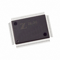
Z8018233FSC Zilog, Z8018233FSC Datasheet - Page 27

Z8018233FSC
Manufacturer Part Number
Z8018233FSC
Description
IC 33MHZ STATIC MIMIC 100-QFP
Manufacturer
Zilog
Datasheet
1.Z8018233FSG.pdf
(109 pages)
Specifications of Z8018233FSC
Processor Type
Z180
Features
Smart Peripheral Controller
Speed
33MHz
Voltage
5V
Mounting Type
Surface Mount
Package / Case
100-QFP
Processor Series
Z8018xx
Core
Z80
Data Bus Width
8 bit
Program Memory Type
ROMLess
Interface Type
UART
Maximum Clock Frequency
33 MHz
Number Of Programmable I/os
24
Number Of Timers
2
Operating Supply Voltage
4.5 V to 5.5 V
Maximum Operating Temperature
+ 70 C
Mounting Style
SMD/SMT
Minimum Operating Temperature
0 C
Lead Free Status / RoHS Status
Contains lead / RoHS non-compliant
Available stocks
Company
Part Number
Manufacturer
Quantity
Price
Company:
Part Number:
Z8018233FSC
Manufacturer:
ZILOG
Quantity:
591
PROGRAMMING
Note:
“x” indicates don’t care condition
DS971820600
PARALLEL PORTS FUNCTIONAL DESCRIPTION
The Z80182/Z8L182 has three 8-bit bi-directional Ports.
Each bit is individually programmable for input or output
(with the exception of PC6 and PC7 which are inputs only).
The following subsections explain and define the
parameters for I/O Address assignments. The three tables
in this section describe the mapping of the common
registers shared by the MPU and the 16550 MIMIC. The
MPU address refers to the I/O address as accessed from
the MPU side (the Z180
MIMIC). Note that only the lowest eight address lines are
decoded for Z182 peripheral access. The full sixteen
Zilog
Register Name
Z80182/Z8L182 MPU Control Registers
Register Name
MMC MIMIC Master Control Register
IUS/IP Interrupt Pending
IE Interrupt Enable
IVEC Interrupt Vector
TTCR Transmit Time Constant
RTCR Receive Time Constant
FSCR FIFO Status and Control
RTTC Receive Timeout Time Constant
TTTC Transmit Timeout Time Constant
RBR Receive Buffer Register
THR Transmit Holding Register
IER Interrupt Enable Register
IIR Interrupt Identification
FCR FIFO Control Register
MM REGISTER
LCR Line Control Register
MCR Modem Control Register
LSR Line Status Register
MSR Modem Status Register
SCR Scratch Register
DLL Divisor Latch (LSByte)
DLM Divisor Latch (MSByte)
™
MPU interface side of the 16550
Table 7. Z80182/Z8L182 MPU Registers
Table 8. Z80182/Z8L182 MIMIC Register MAP
PS009801-0301
P R E L I M I N A R Y
MPU Addr/Access
xxFFH
xxFEH
xxFDH
xxFCH
xxFAH
xxFBH
xxECH
xxEAH
xxEBH
xxF0H
xxF0H
xxF1H
None
xxE9H
XXE9H
xxF3H
xxF4H
xxF5H
xxF6H
xxF7H
xxF8H
xxF9H
MPU Addr
0000H to 00x3FH
(Relocatable to 0040H to 007FH
or 0080H to 00BFH)
The Ports are controlled through two registers: the Port
Direction Control Register and the Port Data Register.
(Please see register description for Ports A, B and C).
address lines are decoded for on-chip Z180 MPU access.
The PC address (coined because the UART is common in
PCs) is the address needed to access the MIMIC registers
through the MIMIC interface signals. The MIMIC interface
signals are multiplexed with the ESCC channel B and the
Port A signals, and must be activated through the System
Configuration Register and the Interrupt Edge/Pin MUX
Register.
R/W
R/Wb7
R/W
R/W
R/W
R/W
R/W7-4
R/W
R/W
W only
R only
R only
R only
W only
R only
R only
R/Wb6432
R/Wb7-4
R only
R only
R only
PC Addr/Access
None
None
None
None
None
None
None
None
None
00H
00H
01H
02H
02H
None
03H
04H
05H
06H
07H
00H
01H
Z
ILOG
DLAB=0 R only
DLAB=0 W only
DLAB=0 R/W
R only
W only
R/W
R/W
R only
R only
R/W
DLAB=1 R/W
DLAB=1 R/W
I
NTELLIGENT
PC Addr
None
Z80182/Z8L182
P
ERIPHERAL
3-27


