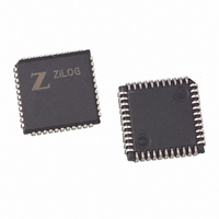
Z8523016VSG Zilog, Z8523016VSG Datasheet - Page 78

Z8523016VSG
Manufacturer Part Number
Z8523016VSG
Description
IC 16MHZ ESCC 44-PLCC
Manufacturer
Zilog
Datasheet
1.Z8523008PSG.pdf
(117 pages)
Specifications of Z8523016VSG
Controller Type
Serial Communications Controller (SCC)
Interface
Bus
Voltage - Supply
4.5 V ~ 5.5 V
Current - Supply
7mA
Operating Temperature
0°C ~ 70°C
Mounting Type
Surface Mount
Package / Case
44-LCC (J-Lead)
Operating Supply Voltage
5 V
Supply Current (max)
9 mA
Maximum Operating Temperature
+ 70 C
Minimum Operating Temperature
0 C
Mounting Style
SMD/SMT
Lead Free Status / RoHS Status
Lead free / RoHS Compliant
Other names
269-3927
Z8523016VSG
Z8523016VSG
Available stocks
Company
Part Number
Manufacturer
Quantity
Price
Company:
Part Number:
Z8523016VSG
Manufacturer:
ZILOG
Quantity:
2 700
Company:
Part Number:
Z8523016VSG
Manufacturer:
ZILOG
Quantity:
2 700
Company:
Part Number:
Z8523016VSG
Manufacturer:
Zilog
Quantity:
231
Part Number:
Z8523016VSG
Manufacturer:
ZILOG
Quantity:
20 000
PS005303-0907
Z85230 Read Cycle Timing
Z85230 Write Cycle Timing
A/B, D/C
from the falling edge of WR or RD in the first transaction involving the ESCC, to the fall-
ing edge of WR or RD in the second transaction. This time must be at least four PCLKs
regardless of which register or channel is accessed.
Figure 20
INTACK must remain stable throughout the cycle. The effective RD time reduces if CE
falls after RD falls, or if it rises before RD rises.
Figure 21
status on INTACK must remain stable throughout the cycle. The effective WR time
reduces if CE falls after WR falls, or if it rises before WR rises. In Write Cycle timing, the
WR signal returns a High slightly before the Address goes invalid.
Because many popular CPUs do not guarantee that the databus is valid when WR is Low,
the ESCC no longer requires a valid databus when the WR pin is Low. For more informa-
tion, see AC characteristics parameter 29 available in
INTACK
D7–D0
RD
CE
illustrates Read Cycle timing. Addresses on A/B and D/C and the status on
on page 74 illustrates Write Cycle timing. Addresses on A/B and D/C and the
Figure 20. Read Cycle Timing (Z85230)
Address Valid
Data Valid
Table
46.
Product Specification
Z80230 Interface Timing
Z85230/Z80230
73


