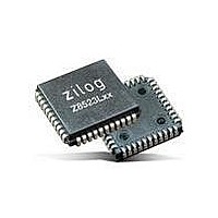
Z8523L16VSG Zilog, Z8523L16VSG Datasheet - Page 9

Z8523L16VSG
Manufacturer Part Number
Z8523L16VSG
Description
IC CTRL SCC 16MHZ 3.3V 44-PLCC
Manufacturer
Zilog
Datasheet
1.Z8523L10VEG.pdf
(118 pages)
Specifications of Z8523L16VSG
Controller Type
Serial Communications Controller (SCC)
Interface
Bus
Voltage - Supply
3 V ~ 3.6 V
Current - Supply
4mA
Operating Temperature
0°C ~ 70°C
Mounting Type
Surface Mount
Package / Case
44-LCC (J-Lead)
Product
I/O Controller
Operating Supply Voltage
- 0.3 V to 7 V
Supply Current (max)
9 mA
Maximum Operating Temperature
+ 70 C
Minimum Operating Temperature
0 C
Mounting Style
SMD/SMT
Lead Free Status / RoHS Status
Lead free / RoHS Compliant
Other names
269-4730
Available stocks
Company
Part Number
Manufacturer
Quantity
Price
Z80230/Z85230/L
Product Specification
4
Pins Common to Both Z85230/L and Z80230
The pin descriptions for pins common to both Z85230/L and Z80230 are provided below:
These pins function as transmitter
CTSA, CTSB (Clear To Send (Inputs, Active Low))—
enables if they are programmed for AUTO ENABLE (WR3 bit 5 is 1), in which case a
Low on each input enables the respective transmitter. If not programmed as AUTO
ENABLE
the pins may be used as general-purpose inputs. These pins are Schmitt-trigger
,
buffered to accommodate slow rise-time inputs. The ESCC detects pulses on these pins
and may interrupt the CPU on both logic level transitions.
These pins function as
DCDA, DCDB (Data Carrier Detect (Inputs, Active Low))—
receiver enables if they are programmed for AUTO ENABLE (WR3 bit 5 is 1); otherwise,
they are used as general-purpose input pins. The pins are Schmitt-trigger buffered to
accommodate slow rise-time signals. The ESCC detects pulses on these pins and may
interrupt the CPU on both logic level transitions.
The RTS pins can be used as
RTSA, RTSB (Request To Send (Outputs, Active Low))—
general-purpose outputs or with the AUTO ENABLE feature. When AUTO-ENABLE is
off, these pins follow the inverse state of WR5 bit 1. When used with the AUTO-
ENABLE feature in ASYNCHRONOUS mode, this pin immediately goes Low when
WR5 bit 1 is 1. When WR5 bit 0 is 0, this pin remains Low until the transmitter is empty.
In Synchronous Data Link Control (SDLC) mode, the RTS pins can be programmed to be
deasserted when the closing flag of the message clears the TxD pin, if WR7’ bit 2 is 1,
WR10 bit 2 is 0, and WR5 bit 1 is 0.
These pins can
SYNCA, SYNCB (Synchronization (Inputs Or Outputs, Active Low))—
act either as inputs, outputs, or as part of the crystal oscillator circuit. In the ASYNCHRO-
NOUS RECEIVE mode (crystal oscillator option not selected), these pins are inputs simi-
lar to CTS and DCD. In this mode, transition on these lines affect the state of the SYNC/
HUNT status bits in Read Register 0 but have no other function.
In EXTERNAL SYNCHRONIZATION mode, with the crystal oscillator not selected,
these lines also act as inputs. In this mode, SYNC is driven Low, two Rx clock cycles after
the last bit of the SYNC character is received. Character assembly begins on the rising
edge of the receive clock immediately preceding the activation of SYNC.
In the INTERNAL SYNCHRONIZATION mode (MONOSYNC and BISYNC) with the
crystal oscillator not selected, these pins act as outputs. These outputs go Low each time a
SYNC pattern is recognized, regardless of character boundaries. In SDLC mode, pins
switch from input to output when MONOSYNC, BISYNC, or SDLC is programmed in
WR4 and SYNC modes are enabled.
DTR/REQA, DTR/REQB (Data Terminal Ready/Request (Output, Active Low))—
These pins can be programmed (WR14 bit 2) to serve either as general-purpose outputs or
as DMA Request lines. When programmed for DTR function (WR14 bit 2 is 0), these out-
puts follow the inverse of the DTR bit of Write Register 5 (WR5 bit 7). When pro-
grammed for REQUEST mode these pins serve as DMA Requests for the transmitter.
PS005308-0609
Pin Descriptions


