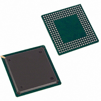
DS31256 Maxim Integrated Products, DS31256 Datasheet - Page 22

DS31256
Manufacturer Part Number
DS31256
Description
IC CTRLR HDLC 256-CHANNEL 256BGA
Manufacturer
Maxim Integrated Products
Datasheet
1.DS31256.pdf
(183 pages)
Specifications of DS31256
Controller Type
HDLC Controller
Interface
Serial
Voltage - Supply
3 V ~ 3.6 V
Current - Supply
500mA
Operating Temperature
0°C ~ 70°C
Mounting Type
Surface Mount
Package / Case
256-BGA
Lead Free Status / RoHS Status
Contains lead / RoHS non-compliant
Available stocks
Company
Part Number
Manufacturer
Quantity
Price
Part Number:
DS31256
Manufacturer:
DALLAS
Quantity:
20 000
3.4 JTAG Signal Description
Signal Name:
Signal Description:
Signal Type:
This signal is used to shift data into JTDI on the rising edge and out of JTDO on the falling edge. If unused, this
signal should be pulled high.
Signal Name:
Signal Description:
Signal Type:
Test instructions and data are clocked into this signal on the rising edge of JTCLK. If unused, this signal should be
pulled high. This signal has an internal pullup.
Signal Name:
Signal Description:
Signal Type:
Test instructions are clocked out of this signal on the falling edge of JTCLK. If unused, this signal should be left
open circuited.
Signal Name:
Signal Description:
Signal Type:
This signal is used to asynchronously reset the test access port controller. At power-up, JTRST must be set low
and then high. This action sets the device into the boundary scan bypass mode, allowing normal device operation.
If boundary scan is not used, this signal should be held low. This signal has an internal pullup.
Signal Name:
Signal Description:
Signal Type:
This signal is sampled on the rising edge of JTCLK and is used to place the test port into the various defined IEEE
1149.1 states. If unused, this signal should be pulled high. This signal has an internal pullup.
3.5 PCI Bus Signal Description
Signal Name:
Signal Description:
Signal Type:
This clock input provides timing for the PCI bus and the device’s internal logic. A 25MHz to 33MHz clock with a
nominal 50% duty cycle should be applied here.
Signal Name:
Signal Description:
Signal Type:
This active-low input is used to force an asynchronous reset to both the PCI bus and the device’s internal logic.
When forced low, this input forces all the internal logic of the device into its default state, forces the PCI outputs
into tri-state, and forces the TD[15:0] output port-data signals high.
Signal Name:
Signal Description:
Signal Type:
Both address and data information are multiplexed onto these signals. Each bus transaction consists of an address
phase followed by one or more data phases. Data can be either read or written in bursts. The address is transferred
during the first clock cycle of a bus transaction. When the Little Endian format is selected, PAD[31:24] is the
MSB of the DWORD; when Big Endian is selected, PAD[7:0] contains the MSB. When the device is an initiator,
JTCLK
JTAG IEEE 1149.1 Test Serial Clock
Input
JTDI
JTAG IEEE 1149.1 Test Serial-Data Input
Input (with internal 10kΩ pullup)
JTDO
JTAG IEEE 1149.1 Test Serial-Data Output
Output
JTRST
JTAG IEEE 1149.1 Test Reset
Input (with internal 10kΩ pullup)
JTMS
JTAG IEEE 1149.1 Test Mode Select
Input (with internal 10kΩ pullup)
PCLK
PCI and System Clock
Input (Schmitt triggered)
PRST
PCI Reset
Input
PAD0 to PAD31
PCI Address and Data Multiplexed Bus
Input/Output (tri-state capable)
22 of 183


