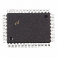
DP83902AVLJ National Semiconductor, DP83902AVLJ Datasheet - Page 10

DP83902AVLJ
Manufacturer Part Number
DP83902AVLJ
Description
IC CTRLR SER NETWORK IN 100PQFP
Manufacturer
National Semiconductor
Datasheet
1.DP83902AVJGNOPB.pdf
(70 pages)
Specifications of DP83902AVLJ
Controller Type
Serial Network Interface Controller
Interface
Serial
Voltage - Supply
4.75 V ~ 5.25 V
Current - Supply
140mA
Operating Temperature
0°C ~ 70°C
Mounting Type
Surface Mount
Package / Case
100-MQFP, 100-PQFP
Lead Free Status / RoHS Status
Contains lead / RoHS non-compliant
Other names
*DP83902AVLJ
Available stocks
Company
Part Number
Manufacturer
Quantity
Price
Company:
Part Number:
DP83902AVLJ
Manufacturer:
NS
Quantity:
2 500
Company:
Part Number:
DP83902AVLJ
Manufacturer:
RAYCHEM
Quantity:
2 500
Company:
Part Number:
DP83902AVLJ
Manufacturer:
Texas Instruments
Quantity:
10 000
Part Number:
DP83902AVLJ
Manufacturer:
NS/国半
Quantity:
20 000
4 0 Functional Description
These four signals are resistively combined TXO
TXOd
pre-emphasis and is required to compensate for the twisted
pair cable which acts like a low pass filter causing greater
attenuation to the 10 MHz (50 ns) pulses of the Manchester
encoded waveform than the 5 MHz (100 ns) pulses
An example of how these signals are combined is shown in
the following diagram
The signal with pre-emphasis shown above is generated by
resistively combining TXO
with its complement is passed to the transmit filter
STATUS INFORMATION
Status information is provided by the ST-NIC on the
CRS RX TXE TX COL and POL outputs as described in
the pin description table These outputs are suitable for driv-
ing status LEDs via an appropriate driver circuit
The POL output is normally low and will be driven high
when seven consecutive link pulses or three consecutive
receive packets are detected with reversed polarity A polar-
ity reversal can be caused by a wiring error at either end of
the TPI cable On detection of a polarity reversal the condi-
tion is latched and POL is asserted The TPI corrects for this
error internally and will decode received data correctly elim-
inating the need to correct the wiring error
ENCODER DECODER (ENDEC) MODULE
The ENDEC consists of three main logical blocks
a) The Manchester encoder accepts NRZ data from the
b) The Manchester decoder receives Manchester data from
c) The collision translator indicates to the controller the
MANCHESTER ENCODER AND DIFFERENTIAL DRIVER
The differential transmit pair on the secondary of the trans-
former drives up to 50 meters of twisted pair AUI cable
These outputs are source followers which require two 270
pull-down resistors to ground
The DP83902A allows both half-step and full-step to be
compatible with Ethernet and IEEE 802 3 With the SEL pin
low (for Ethernet I) Transmit
controller encodes the data to Manchester and trans-
mits it differentially to the transceiver through the differ-
ential transmit driver
the transceiver converts it to NRZ data and clock pulses
and sends it to the controller
presence of a valid 10 MHz collision signal to the PLL
b
and TXO
b
with TXOd
a
and TXOd
a
a
is positive with respect to
This is known as digital
b
This signal along
(Continued)
TL F 11157–6
a
with
10
Transmit
Transmit
provides zero differential voltage to operate with transform-
er coupled loads
MANCHESTER DECODER
The decoder consists of a differential receiver and a PLL to
separate a Manchester decoded data stream into internal
clock signals and data The differential input must be exter-
nally terminated with two 39
if the standard 78
Ethernet applications these resistors are optional To pre-
vent noise from falsely triggering the decoder a squelch
circuit at the input rejects signals with levels less than
b
coded Data becomes valid typically within 5 bit times The
DP83902A may tolerate bit jitter up to 18 ns in the received
data The decoder detects the end of a frame when no more
mid-bit transitions are detected
COLLISION TRANSLATOR
When in AUI mode when the Ethernet transceiver (DP8392
CTI) detects a collision it generates a 10 MHz signal to the
differential collision inputs (CD
these inputs are detected active the DP83902A uses this
signal to back off its current transmission and reschedule
another one
The collision differential inputs are terminated the same way
as the differential receive inputs The squelch circuitry is
also similar rejecting pulses with levels less than
CRYSTAL OSCILLATOR OPERATION
OCSILLATOR
The oscillator is controlled by a 20 MHz parallel resonant
crystal connected between X1 and X2 or by an external
clock on X1 The 20 MHz output of the oscillator is divided
by 2 to generate the 10 MHz transmit clock for the control-
ler The oscillator also provides internal clock signals to the
encoding and decoding circuits
Note When X1 is being driven by an external oscillator X2 MUST be
The 20 MHz crystal connection to the DP83902 requires
special care The IEEE 802 3 standard requires the trans-
mitted signal frequency to be accurate within
Stray capacitance can shift the crystal’s frequency out of
range and cause transmitted frequency to exceed its 0 01%
tolerance The frequency marked on the crystal is usually
measured with a fixed load capacitance specified in the
crystal’s data sheet typically 20 pF
Resonant Frequency
Tolerance
Stability
Type
Circuit
Max ESR
Crystal Load Capacitor
175 mV Signals more negative than
grounded
b
a
and Transmit
during idle with SEL high (for IEEE 802 3)
Crystal Specifications
transceiver drop cable is used In thin
b
are equal in the idle state This
resistors connected in series
20 MHz
AT Cut
Parallel Resonance
25
20 pF
g
g
g
) of the DP83902A When
0 005% at 25 C
0 005% at 0 C– 70 C
b
300 mV are de-
b
g
175 mV
0 01%


