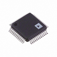
AD9951YSVZ Analog Devices Inc, AD9951YSVZ Datasheet - Page 16

AD9951YSVZ
Manufacturer Part Number
AD9951YSVZ
Description
IC DDS DAC 14BIT 1.8V 48-TQFP
Manufacturer
Analog Devices Inc
Specifications of AD9951YSVZ
Resolution (bits)
14 b
Master Fclk
400MHz
Tuning Word Width (bits)
32 b
Voltage - Supply
1.71 V ~ 1.96 V
Operating Temperature
-40°C ~ 105°C
Mounting Type
Surface Mount
Package / Case
48-TQFP Exposed Pad, 48-eTQFP, 48-HTQFP, 48-VQFP
Data Rate
25Mbps
Rf Ic Case Style
TQFP
No. Of Pins
48
Supply Voltage Range
1.8V To 3.3V
Operating Temperature Range
-40°C To +105°C
Msl
MSL 3 - 168 Hours
Ic Function
Direct Digital Synthesizer
Digital Ic Case Style
TQFP
Svhc
No SVHC (15-Dec-2010)
Rohs Compliant
Yes
Termination Type
SMD
Ic Generic Number
9951
Base Number
9951
Filter Terminals
SMD
Lead Free Status / RoHS Status
Lead free / RoHS Compliant
For Use With
AD9951/PCB - BOARD EVAL FOR AD9951
Lead Free Status / Rohs Status
Compliant
Available stocks
Company
Part Number
Manufacturer
Quantity
Price
Company:
Part Number:
AD9951YSVZ
Manufacturer:
AD
Quantity:
1 300
Company:
Part Number:
AD9951YSVZ
Manufacturer:
ADI
Quantity:
102
Company:
Part Number:
AD9951YSVZ
Manufacturer:
ADI
Quantity:
650
Company:
Part Number:
AD9951YSVZ
Manufacturer:
Analog Devices Inc
Quantity:
10 000
AD9951
CFR1<6>: Not Used
CFR1<5>: DAC Power-Down Bit
CFR1<5> = 0 (default). The DAC is enabled for operation.
CFR1<5> = 1. The DAC is disabled and is in its lowest power
dissipation state.
CFR1<4>: Clock Input Power-Down Bit
CFR1<4> = 0 (default). The clock input circuitry is enabled for
operation.
CFR1<4> = 1. The clock input circuitry is disabled and the
device is in its lowest power dissipation state.
CFR1<3>: External Power-Down Mode
CFR1<3> = 0 (default). The external power-down mode
selected is the rapid recovery power-down mode. In this mode,
when the PWRDWNCTL input pin is high, the digital logic
and the DAC digital logic are powered down. The DAC bias
circuitry, PLL, oscillator, and clock input circuitry are not
powered down.
CFR1<3> = 1. The external power-down mode selected is the
full power-down mode. In this mode, when the PWRDWNCTL
input pin is high, all functions are powered down. This includes
the DAC and PLL, which take a significant amount of time to
power up.
CFR1<2>: Not Used
CFR1<1>: SYNC_CLK Disable Bit
CFR1<1> = 0 (default). The SYNC_CLK pin is active.
CFR1<1> = 1. The SYNC_CLK pin assumes a static Logic 0
state to keep noise generated by the digital circuitry at a mini-
mum. However, the synchronization circuitry remains active
(internally) to maintain normal device timing.
CFR1<0>: Not Used, Leave at 0
Control Function Register No. 2 (CFR2)
The CFR2 is used to control the various functions, features, and
modes of the AD9951, primarily related to the analog sections
of the chip.
CFR2<23:12>: Not Used
CFR2<11>: High Speed Sync Enable Bit
CFR2<11> = 0 (default). The high speed sync enhancement is off.
Rev. 0 | Page 16 of 28
CFR2<11> = 1. The high speed sync enhancement is on. This
bit should be set when attempting to use the auto-
synchronization feature for SYNC_CLK inputs beyond 50 MHz,
(200 MSPS SYSCLK). See the Synchronizing Multiple AD9951s
section for details.
CFR2<10>: Hardware Manual Sync Enable Bit
CFR2<10> = 0 (default). The hardware manual sync function is off.
CFR2<10> = 1. The hardware manual sync function is enabled.
While this bit is set, a rising edge on the SYNC_IN pin will
cause the device to advance the SYNC_CLK rising edge by one
REFCLK cycle. Unlike the software manual sync enable bit, this
bit does not self-clear. Once the hardware manual sync mode is
enabled, it will stay enabled until this bit is cleared. See the
Synchronizing Multiple AD9951s section for details.
CFR2<9>: CRYSTAL OUT Enable Bit
CFR2<9> = 0 (default). The CRYSTAL OUT pin is inactive.
CFR2<9> = 1. The CRYSTAL OUT pin is active. When active,
the crystal oscillator circuitry output drives the CRYSTAL OUT
pin, which can be connected to other devices to produce a refer-
ence frequency. The oscillator will respond to crystals in the
range of 20 MHz to 30 MHz.
CFR2<8>: Not Used
CFR2<7:3>: Reference Clock Multiplier Control Bits
This 5-bit word controls the multiplier value out of the clock-
multiplier (PLL) block. Valid values are decimal 4 to 20 (0x04 to
0x14). Values entered outside this range will bypass the clock
multiplier. See the Phase-Locked Loop (PLL) section for details.
CFR2<2>: VCO Range Control Bit
This bit is used to control the range setting on the VCO.
When CFR2<2> == 0 (default), the VCO operates in a range of
100 MHz to 250 MHz. When CFR2<2> == 1, the VCO operates
in a range of 250 MHz to 400 MHz.
CFR2<1:0>: Charge Pump Current Control Bits
These bits are used to control the current setting on the charge
pump. The default setting, CFR2<1:0>, sets the charge pump
current to the default value of 75 µA. For each bit added (01, 10,
11), 25 µA of current is added to the charge pump current:
100 µA, 125 µA, and 150 µA.


