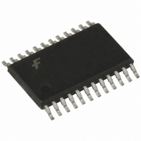
74LVX4245MTC Fairchild Semiconductor, 74LVX4245MTC Datasheet - Page 4

74LVX4245MTC
Manufacturer Part Number
74LVX4245MTC
Description
TXRX 8-BIT DUAL 3STATE 24TSSOP
Manufacturer
Fairchild Semiconductor
Series
74LVXr
Type
Transceiverr
Datasheet
1.74LVX4245MTCX.pdf
(8 pages)
Specifications of 74LVX4245MTC
Number Of Drivers/receivers
8/8
Voltage - Supply
2.7 V ~ 5.5 V
Mounting Type
Surface Mount
Package / Case
24-TSSOP
Logic Type
CMOS
Logic Family
74LVX
Number Of Channels Per Chip
8
Input Level
CMOS
Output Level
CMOS
Output Type
3-State
High Level Output Current
- 24 mA
Low Level Output Current
24 mA
Propagation Delay Time
8.5 ns
Supply Voltage (max)
3.6 V, 5.5 V
Supply Voltage (min)
2.7 V, 4.5 V
Maximum Operating Temperature
+ 85 C
Function
Transceiver
Input Bias Current (max)
8 uA
Minimum Operating Temperature
- 40 C
Mounting Style
SMD/SMT
Number Of Circuits
2
Polarity
Non-Inverting
Output Current
50mA
Supply Voltage Range
2.7V To 5.5V
Logic Case Style
TSSOP
No. Of Pins
24
Operating Temperature Range
-40°C To +85°C
Rohs Compliant
Yes
Lead Free Status / RoHS Status
Lead free / RoHS Compliant
Protocol
-
Lead Free Status / Rohs Status
Lead free / RoHS Compliant
Available stocks
Company
Part Number
Manufacturer
Quantity
Price
Part Number:
74LVX4245MTC
Manufacturer:
FAIRCHILD/仙童
Quantity:
20 000
Company:
Part Number:
74LVX4245MTCX
Manufacturer:
FSC
Quantity:
5 000
Part Number:
74LVX4245MTCX
Manufacturer:
FAIRCHILD/仙童
Quantity:
20 000
www.fairchildsemi.com
t
t
t
t
t
t
t
t
t
t
t
t
t
t
I
I
V
V
V
V
V
V
V
V
PHL
PLH
PHL
PLH
PZL
PZH
PZL
PZH
PHZ
PLZ
PHZ
PLZ
OSHL
OSLH
CCA
CCB
Symbol
DC Electrical Characteristics
Note 3: Maximum test duration 2.0 ms, one output loaded at a time.
Note 4: Worst case package.
Note 5: Max number of outputs defined as (n). Data inputs are driven 0V to V
Note 6: Max number of Data Inputs (n) switching. (n 1) inputs switching 0V to V
AC Electrical Characteristics
Note 7: Voltage Range 5.0V is 5.0V
Note 8: Voltage Range 3.3V is 3.3V
Note 9: Skew is defined as the absolute value of the difference between the actual propagation delay for any two separate outputs of the same device. The
specification applies to any outputs switching in the same direction, either HIGH-to-LOW (t
OLPA
OLPB
OLVA
OLVB
IHDA
IHDB
ILDA
ILDB
Symbol
V
Quiescent V
Supply Current
Quiescent V
Supply Current
Quiet Output Maximum
Dynamic V
Quiet Output Minimum
Dynamic V
Minimum HIGH Level
Dynamic Input Voltage
Maximum LOW Level
Dynamic Input Voltage
CC
Propagation Delay
A to B
Propagation Delay
B to A
Output Enable Time
OE to B
Output Enable Time
OE to A
Output Disable Time
OE to B
Output Disable Time
OE to A
Output to Output
Skew (Note 9)
Data to Output
level to threshold (V
OL
OL
Parameter
CCA
CCB
Parameters
IHD
0.5V.
0.3V.
), OV to threshold (V
V
(V)
5.5
5.5
5.0
5.0
5.0
5.0
5.0
5.0
5.0
5.0
CCA
ILD
Min
1.0
1.0
1.0
1.0
1.0
1.0
1.0
1.0
1.0
1.0
1.0
1.0
), f
(Continued)
V
V
CCB
V
CCA
3.6
3.6
3.3
3.3
3.3
3.3
3.3
3.3
3.3
3.3
(V)
1 MHz.
CCB
T
C
A
L
3.3V (Note 8)
5V (Note 7)
Typ
5.1
5.3
5.4
5.5
6.5
6.7
5.2
5.8
6.0
3.3
3.9
2.9
1.0
50 pF
25 C
CC
4
Typ
CC
level; one output at GND.
T
level. Input-under-test switching:
A
Max
10.0
10.0
8.5
8.5
8.5
8.5
9.0
9.0
9.5
6.5
7.0
6.5
1.5
25 C
OSHL
1.5
0.8
2.0
2.0
0.8
0.8
1.2
0.8
8
5
) or LOW-to-HIGH (t
Guaranteed Limits
V
T
V
CCB
A
CCA
Min
1.0
1.0
1.0
1.0
1.0
1.0
1.0
1.0
1.0
1.0
1.0
1.0
T
C
A
40 C to 85 C T
L
3.3V (Note 8)
5V (Note 7)
50 pF
40 C to 85 C
80
50
Max
10.5
10.5
10.0
9.0
9.0
9.0
9.0
9.5
9.5
7.0
7.5
7.0
1.5
OSLH
). Parameter guaranteed by design.
V
A
CCA
Min
1.0
1.0
1.0
1.0
1.0
1.0
1.0
1.0
1.0
1.0
1.0
1.0
Units
V
C
CCB
V
V
V
V
40 C to 85 C
L
A
A
5V (Note 7)
50 pF
A
B
OE
A
B
OE
(Note 4)(Note 5)
(Note 4)(Note 5)
(Note 4)(Note 6)
(Note 4)(Note 6)
2.7V
n
n
n
n
Max
10.0
10.0
10.0
10.0
10.0
10.0
10.0
11.5
11.5
7.5
7.5
7.5
1.5
V
V
V
V
Conditions
GND T/R
GND T/R
CCA
CCB
CCA
CCB
or GND
or GND,
or GND
or GND,
Units
ns
ns
ns
ns
ns
ns
ns
GND
V
CCA


