DS14185WM/NOPB National Semiconductor, DS14185WM/NOPB Datasheet - Page 3
DS14185WM/NOPB
Manufacturer Part Number
DS14185WM/NOPB
Description
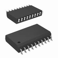
IC DVR/RCVR EIA/TIA-232 20-SOIC
Manufacturer
National Semiconductor
Type
Transceiverr
Datasheet
1.DS14185WM.pdf
(8 pages)
Specifications of DS14185WM/NOPB
Number Of Drivers/receivers
3/5
Protocol
RS232
Voltage - Supply
4.75 V ~ 5.25 V
Mounting Type
Surface Mount
Package / Case
20-SOIC (7.5mm Width)
Lead Free Status / RoHS Status
Lead free / RoHS Compliant
Other names
*DS14185WM/NOPB


DRIVER CHARACTERISTICS
R
RECEIVER CHARACTERISTICS
V
V
R
I
V
V
I
IN
OSR
Symbol
O
TH
TL
IN
OH
OL
DRIVER CHARACTERISTICS
t
t
t
RECEIVER CHARACTERISTICS
t
t
t
t
Electrical Characteristics
Symbol
Over recommended supply voltage and operating temperature ranges, unless otherwise specified.
Switching Characteristics
PHL
PLH
r
PHL
PLH
r
f
Note 1: Absolute Maximum Ratings are those values beyond which the safety of the device cannot be guaranteed. They are not meant to imply that the devices
should be operated at these limits. The table of Electrical Characteristics specifies conditions of device operation.
Note 2: Current into device pins is defined as positive. Current out of device pins is defined as negative. All voltages are referenced to ground unless otherwise
specified. For current, minimum and maximum values are specified as an absolute value and the sign is used to indicate direction. For voltage logic levels, the more
positive value is designated as maximum. For example, if −6V is a maximum, the typical value (−6.8V) is more negative.
Note 3: All typicals are given for: V
Note 4: Only one driver output shorted at a time.
Note 5: Generator characteristics for driver input: f = 64 kHz (128 kbits/sec), t
Note 6: Generator characteristics for receiver input: f = 64 kHz (128 kbits/sec), t
Note 7: If receiver inputs are unconnected, receiver output is a logic high.
Note 8: Refer to typical curves. Driver output slew rate is measured from the +3.0V to the −3.0V level on the output waveform. Inputs not under test are connected
to V
, t
T
A
f
CC
= 25˚C
or GND. Slew rate is determined by load capacitance. To comply with a 30 V/µs maximum slew rate, a minimum load capacitance of 390 pF is recommended.
Output Resistance
Input High Threshold
(Recognized as a High Signal)
Input Low Threshold
(Recognized as a Low Signal)
Input Resistance
Input Current (Note 2)
High Level Output Voltage
Low Level Output Voltage
Short Circuit Current (Note 2)
Propagation Delay High to Low
Propagation Delay Low to High
Output Slew Rate (Note 8)
Propagation Delay High to Low
Propagation Delay Low to High
Rise Time
Fall Time
Parameter
(Note 7)
Parameter
CC
= +5.0V, V
+
= +12.0V, V
(Note 2) (Continued)
−2V ≤ V
V
−2V ≤ V
V
V
V
V
V
V
V
V
I
I
I
I
I
V
(Note 2)
OH
OH
OH
OH
OL
+
+
O
O
IN
IN
IN
IN
IN
O
= V
= V
≤ 0.4V, I
≥ 2.5V, I
= 3.2 mA, V
= 0V, V
=
= +15V
= +3V
= −15V
= −3V
= −0.5 mA, V
= −10 µA, V
= −0.5 mA, V
= −10 µA, V
−
±
−
−
R
(Figures 1, 2)
R
(includes fixture plus probe),
(Figures 3, 4)
= −12V, T
3V to
O
O
= V
= V
L
L
≤ +2V,
≤ +2V,
= 3 kΩ, C
= 1.5 kΩ, C
IN
CC
CC
O
O
= 0V
±
= 3.2 mA
= −0.5 mA
A
= 0V
= Open Ckt
15V
IN
IN
IN
= +25˚C.
IN
IN
r
Conditions
= +3V
= −3V
= Open Circuit
= t
3
r
= −3V
= Open Circuit
L
= t
f
Conditions
<
= 50 pF
L
f
= 200 ns, V
10 ns, V
= 15 pF
IH
= 3V, V
IH
= 3V, V
IL
= 0V, duty cycle = 50%.
IL
= −3V, duty cycle = 50%.
Min
0.43
−5.0
Typ
240
150
240
Min
300
300
0.7
3.0
2.1
2.6
4.0
2.6
4.0
60
50
87
40
−1
−4
−0.65 −0.43
1.85
−4.1
−2.7
Typ
1.0
4.1
4.1
0.7
4.9
4.9
0.2
4
4
Max
350
350
350
350
175
100
www.national.com
Max
−2.1
−1.7
2.4
7.0
5.0
0.4
1
Units
Units
ns
ns
ns
ns
ns
ns
ns
mA
mA
mA
mA
mA
kΩ
Ω
Ω
V
V
V
V
V
V
V
Related parts for DS14185WM/NOPB
Image
Part Number
Description
Manufacturer
Datasheet
Request
R

Part Number:
Description:
IC DVR/RCVR EIA/TIA-232 20-SOIC
Manufacturer:
National Semiconductor
Datasheet:
Part Number:
Description:
National Semiconductor [8-Bit D/A Converter]
Manufacturer:
National Semiconductor
Datasheet:
Part Number:
Description:
National Semiconductor [Media Coprocessor]
Manufacturer:
National Semiconductor
Datasheet:
Part Number:
Description:
Digitally Controlled Tone and Volume Circuit with Stereo Audio Power Amplifier, Microphone Preamp Stage and National 3D Sound
Manufacturer:
National Semiconductor
Datasheet:
Part Number:
Description:
Digitally Controlled Tone and Volume Circuit with Stereo Audio Power Amplifier, Microphone Preamp Stage and National 3D Sound
Manufacturer:
National Semiconductor
Datasheet:
Part Number:
Description:
AC97 Rev 2 Codec with Sample Rate Conversion and National 3D Sound
Manufacturer:
National Semiconductor
Part Number:
Description:
Manufacturer:
National Semiconductor
Datasheet:
Part Number:
Description:
Manufacturer:
National Semiconductor
Datasheet:
Part Number:
Description:
General Purpose, Low Voltage, Low Power, Rail-to-Rail Output Operational Amplifiers
Manufacturer:
National Semiconductor
Datasheet:
Part Number:
Description:
8-bit 20 MSPS flash A/D converter.
Manufacturer:
National Semiconductor
Datasheet:
Part Number:
Description:
Low Noise Quad Operational Amplifier
Manufacturer:
National Semiconductor
Datasheet:
Part Number:
Description:
Quad Differential Line Receivers
Manufacturer:
National Semiconductor
Datasheet:
Part Number:
Description:
Quad High Speed Trapezoidal? Bus Transceiver
Manufacturer:
National Semiconductor
Datasheet:
Part Number:
Description:
Dual Line Receiver
Manufacturer:
National Semiconductor
Datasheet: