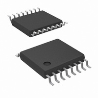
DS90LV049TMT/NOPB National Semiconductor, DS90LV049TMT/NOPB Datasheet

DS90LV049TMT/NOPB
Specifications of DS90LV049TMT/NOPB
*DS90LV049TMT/NOPB
DS90LV049TMT
Available stocks
Related parts for DS90LV049TMT/NOPB
DS90LV049TMT/NOPB Summary of contents
Page 1
... Order Number DS90LV049TMTX (Tape and Reel) See NS Package Number MTC16 Truth Table Open Open H © 2005 National Semiconductor Corporation Features 400 Mbps switching rates n Flow-through pinout simplifies PCB layout typical driver channel-to-channel skew typical receiver channel-to-channel skew n 3.3 V single power supply design n TRI-STATE output control n Internal fail-safe biasing of receiver inputs n Low power dissipation ( ...
Page 2
... Absolute Maximum Ratings If Military/Aerospace specified devices are required, please contact the National Semiconductor Sales Office/ Distributors for availability and specifications. Supply Voltage ( LVCMOS Input Voltage ( LVDS Input Voltage ( IN+ IN- Enable Input Voltage (EN, EN) LVCMOS Output Voltage (R ) OUT LVDS Output Voltage ( OUT+ ...
Page 3
Electrical Characteristics Over supply voltage and operating temperature ranges, unless otherwise specified. (Notes Symbol Parameter LVCMOS Output DC Specifications (Receiver Outputs) V Output High Voltage OH V Output Low Voltage OL I Output TRI-STATE Current OZ General ...
Page 4
Switching Characteristics Note differential channel-to-channel skew is defined as the magnitude difference in the differential propagation delays between two driver channels on SKD2 the same device. Note differential part-to-part skew is defined as |t ...
Page 5
Parameter Measurement Information FIGURE 3. Driver Propagation Delay and Transition Time Waveforms FIGURE 4. Driver TRI-STATE Delay Test Circuit (Continued) 20042005 5 20042006 www.national.com ...
Page 6
Parameter Measurement Information FIGURE 6. Receiver Propagation Delay and Transition Time Test Circuit FIGURE 7. Receiver Propagation Delay and Transition Time Waveforms www.national.com (Continued) FIGURE 5. Driver TRI-STATE Delay Waveform 6 20042007 20042009 20042010 ...
Page 7
Parameter Measurement Information FIGURE 8. Receiver TRI-STATE Delay Test Circuit FIGURE 9. Receiver TRI-STATE Delay Waveforms Typical Application (Continued) FIGURE 10. Point-to-Point Application 7 20042011 20042014 20042008 www.national.com ...
Page 8
Applications Information General application guidelines and hints for LVDS drivers and receivers may be found in the following application notes: LVDS Owner’s Manual (lit #550062-002), AN-805, AN-808, AN-903, AN-916, AN-971, AN-977. LVDS drivers and receivers are intended to be primarily ...
Page 9
Applications Information The receiver’s internal fail-safe circuitry is designed to source/sink a small amount of current, providing fail-safe protection (a stable known state of HIGH output voltage) for floating receiver inputs. The DS90LV049 has two receivers, and if an application ...
Page 10
... BANNED SUBSTANCE COMPLIANCE National Semiconductor certifies that the products and packing materials meet the provisions of the Customer Products Stewardship Specification (CSP-9-111C2) and the Banned Substances and Materials of Interest Specification (CSP-9-111S2) and contain no ‘‘Banned Substances’’ as defined in CSP-9-111S2. ...


