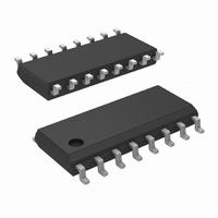
DS90LV047ATMTC/NOPB National Semiconductor, DS90LV047ATMTC/NOPB Datasheet

DS90LV047ATMTC/NOPB
Specifications of DS90LV047ATMTC/NOPB
*DS90LV047ATMTC/NOPB
DS90LV047ATMTC
DS90LV047ATMTC/DRSN
DS90LV047ATMTC/DRSN
Related parts for DS90LV047ATMTC/NOPB
DS90LV047ATMTC/NOPB Summary of contents
Page 1
... L or Open L H All other combinations of X ENABLE inputs TRI-STATE ® registered trademark of National Semiconductor Corporation. © 2003 National Semiconductor Corporation Features > 400 Mbps (200 MHz) switching rates n n Flow-through pinout simplifies PCB layout n 300 ps typical differential skew n 400 ps maximum differential skew n 1 ...
Page 2
... Absolute Maximum Ratings If Military/Aerospace specified devices are required, please contact the National Semiconductor Sales Office/ Distributors for availability and specifications. Supply Voltage ( Input Voltage ( Enable Input Voltage (EN Output Voltage ( OUT+ OUT− Short Circuit Duration ( OUT+ OUT− Maximum Package Power Dissipation ...
Page 3
Switching Characteristics ± +3.3V 10 −40˚C to +85˚C (Notes Symbol Parameter t Differential Propagation Delay High to Low PHLD t Differential Propagation Delay Low to High PLHD t Differential Pulse Skew ...
Page 4
Parameter Measurement Information FIGURE 2. Driver Propagation Delay and Transition Time Test Circuit FIGURE 3. Driver Propagation Delay and Transition Time Waveforms www.national.com (Continued) FIGURE 4. Driver TRI-STATE Delay Test Circuit 4 10088704 10088705 10088706 ...
Page 5
Parameter Measurement Information Typical Application Applications Information General application guidelines and hints for LVDS drivers and receivers may be found in the following application notes: LVDS Owner’s Manual (lit #550062-001), AN808, AN977, AN971, AN916, AN805, AN903. LVDS drivers and receivers ...
Page 6
Typical Application (Continued) is due to the overlap current that flows between the rails of the device when the internal gates switch. Whereas the current mode driver switches a fixed current between its output without any substantial overlap current. This ...
Page 7
Typical Application (Continued) 1. Open Input Pins. The DS90LV048A is a quad receiver device, and if an application requires only receivers, the unused channel(s) inputs should be left OPEN. Do not tie unused receiver inputs to ...
Page 8
Typical Performance Curves Output High Voltage vs Power Supply Voltage Output Short Circuit Current vs Power Supply Voltage Differential Output Voltage vs Power Supply Voltage www.national.com 10088714 Output TRI-STATE Current vs 10088716 Differential Output Voltage 10088718 8 Output Low Voltage ...
Page 9
Typical Performance Curves Offset Voltage vs Power Suppy Voltage Power Supply Current vs Power Supply Voltage Differential Propagation Delay vs Power Supply Voltage (Continued) 10088720 10088722 Differential Propagation Delay vs 10088724 9 Power Supply Current vs Frequency 10088721 Power Supply ...
Page 10
Typical Performance Curves Differential Skew vs Power Supply Voltage Transition Time vs Power Supply Voltage www.national.com (Continued) 10088726 10088728 10 Differential Skew vs Ambient Temperature 10088727 Transition Time vs Ambient Temperature 10088729 ...
Page 11
Typical Performance Curves (Continued) Data Rate vs Cable Length DATA RATE VS CABLE LENGTH GRAPH TEST PROCEDURE A pseudo-random bit sequence (PRBS programmed into a function generator (Tektronix HFS9009) and connected to the driver inputs via 50Ω cables ...
Page 12
Physical Dimensions unless otherwise noted 16-Lead (0.150" Wide) Molded Small Outline Package, JEDEC www.national.com inches (millimeters) Order Number DS90LV047ATM NS Package Number M16A 12 ...
Page 13
... NATIONAL’S PRODUCTS ARE NOT AUTHORIZED FOR USE AS CRITICAL COMPONENTS IN LIFE SUPPORT DEVICES OR SYSTEMS WITHOUT THE EXPRESS WRITTEN APPROVAL OF THE PRESIDENT AND GENERAL COUNSEL OF NATIONAL SEMICONDUCTOR CORPORATION. As used herein: 1. Life support devices or systems are devices or systems which, (a) are intended for surgical implant ...


