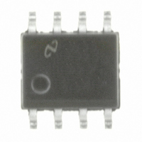
CLC005AJE/NOPB National Semiconductor, CLC005AJE/NOPB Datasheet

CLC005AJE/NOPB
Specifications of CLC005AJE/NOPB
*CLC005AJE/NOPB
CLC005AJE
Related parts for CLC005AJE/NOPB
CLC005AJE/NOPB Summary of contents
Page 1
... CLC005 an excellent general purpose high speed driver for digital applications. The CLC005 is powered from a single +5V or −5.2V supply and comes in an 8-pin SOIC package. Typical Application © 2000 National Semiconductor Corporation Key Specifications n 650 ps rise and fall times n Data rates to 622 Mbps transmis- ...
Page 2
Typical Performance Characteristic Connection Diagram (8-Pin SOIC) www.national.com DS100144-1 DS100144-3 Order Number CLC005AJE See NS Package Number M08A 2 ...
Page 3
... Absolute Maximum Ratings If Military/Aerospace specified devices are required, please contact the National Semiconductor Sales Office/ Distributors for availability and specifications. Supply Voltage Output Current Maximum Junction Temperature Storage Temperature Range Lead Temperature (Soldering 10 seconds) ESD Rating (Human Body Model) Electrical Characteristics ...
Page 4
Operation INPUT INTERFACING The CLC005 has high impedance, emitter-follower buffered, differential inputs. Single-ended signals may also be input. Transmission lines supplying input signals must be properly terminated close to the CLC005. Either A.C. or D.C. coupling as in Figure 2 ...
Page 5
Operation (Continued) FIGURE 4. Single Ended 50 FIGURE 5. Differential 50 FIGURE 3. DC Coupled Input OUTPUT INTERFACING The CLC005’s class AB output stage, Figure 6 , requires no standing current in the output transistors and therefore re- quires no ...
Page 6
Operation (Continued) OUTPUT AMPLITUDE ADJUSTMENT The high and low output levels of the CLC005 are set by a circuit shown simplified in Figure 8 . Output high and low lev- els may be set independently with external resistor networks connected ...
Page 7
Operation (Continued) FIGURE 10. Resistance Pins Output Voltage FIGURE 11. Differential Input Increased Output FIGURE 9. Differential Input Reduced Output Reduced Output @ 150 Load 7 DS100144-12 DS100144-13 DS100144-14 www.national.com ...
Page 8
Operation (Continued) FIGURE 12. Resistance Pins Output Voltage @ Increased Output 150 OUTPUT RISE AND FALL TIMES Output load capacitance can significantly affect output rise and fall times. The effect of load capacitance, stray or other- ...
Page 9
... National Semi- conductor. To order this evaluation board, part number CLC730056, contact your local sales representative or the National Semiconductor Customer Response Center in your area. (This evaluation board is identical to that for the CLC007 for which some of the listed parts are not re- quired ...
Page 10
PCB Layout Recommendations Item Reference Designator 1 C1, C2, C8 C5, C60 3 C7, C10, C13, C14 4 C11, C12 R6,R7 10 R11 11 R12 ...
Page 11
PCB Layout Recommendations (Continued) DS100144-18 DS100144-20 11 DS100144-19 DS100144-21 www.national.com ...
Page 12
... NATIONAL’S PRODUCTS ARE NOT AUTHORIZED FOR USE AS CRITICAL COMPONENTS IN LIFE SUPPORT DEVICES OR SYSTEMS WITHOUT THE EXPRESS WRITTEN APPROVAL OF THE PRESIDENT AND GENERAL COUNSEL OF NATIONAL SEMICONDUCTOR CORPORATION. As used herein: 1. Life support devices or systems are devices or systems which, (a) are intended for surgical implant ...


