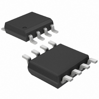
MAX13444EASA+ Maxim Integrated Products, MAX13444EASA+ Datasheet - Page 2

MAX13444EASA+
Manufacturer Part Number
MAX13444EASA+
Description
IC TXRX J1708 HALF DUPLEX 8-SOIC
Manufacturer
Maxim Integrated Products
Type
Transceiverr
Datasheet
1.MAX13442EASA.pdf
(18 pages)
Specifications of MAX13444EASA+
Number Of Drivers/receivers
1/1
Protocol
RS422, RS485
Voltage - Supply
4.75 V ~ 5.25 V
Mounting Type
Surface Mount
Package / Case
8-SOIC (3.9mm Width)
Operating Supply Voltage
1.62 V to 5.5 V
Supply Current
2 mA
Operating Temperature Range
- 40 C to + 85 C
Data Rate
16 Mbps
Mounting Style
SMD/SMT
Propagation Delay Time Ns
50 ns
Lead Free Status / RoHS Status
Lead free / RoHS Compliant
ABSOLUTE MAXIMUM RATINGS
(Voltages referenced to GND.)
V
RE, DE, DE, DI, TXD ...................................-0.3V to (V
A, B (Note 1) (MAX13442E/MAX13444E) ............................±80V
A, B (Note 1) (MAX13443E) .................................................±60V
RO ..............................................................-0.3V to (V
Short-Circuit Duration (RO, A, B) ...............................Continuous
±15kV ESD-Protected, ±80V Fault-Protected,
Fail-Safe RS-485/J1708 Transceivers
PACKAGE THERMAL CHARACTERISTICS (Note 2)
SO
DC ELECTRICAL CHARACTERISTICS
(V
Note 1: During normal operation, a termination resistor must be connected between A and B in order to guarantee overvoltage pro-
Stresses beyond those listed under “Absolute Maximum Ratings” may cause permanent damage to the device. These are stress ratings only, and functional
operation of the device at these or any other conditions beyond those indicated in the operational sections of the specifications is not implied. Exposure to
absolute maximum rating conditions for extended periods may affect device reliability.
2
Note 2: Package thermal resistances were obtained using the method described in JEDEC specification JESD51-7, using a four-
DRIVER
Differential Driver Output
Change in Magnitude of
Differential Output Voltage
Driver Common-Mode
Output Voltage
Change in Magnitude of
Common-Mode Voltage
DRIVER LOGIC
Driver-Input High Voltage
Driver-Input Low Voltage
Driver-Input Current
Driver Short-Circuit Output Current
(Note 4)
Driver Short-Circuit Foldback
Output Current
Driver-Limit Short-Circuit Foldback
Output Current
CC
CC
Junction-to-Ambient Thermal Resistance (θ
Junction-to-Case Thermal Resistance (θ
_______________________________________________________________________________________
........................................................................................+7V
= +4.75V to +5.25V, T
tection up to the absolute maximum rating of this device. When not in operation, these devices can withstand fault voltages
up to the maximum rating without a termination resistor and will not be damaged.
layer board. For detailed information on package thermal considerations, refer to www.maxim-ic.com/thermal-tutorial.
PARAMETER
A
= T
MIN
to T
SYMBOL
I
I
I
V
OSDF
OSDL
MAX
V
V
V
I
OSD
V
V
DIN
DIH
DIL
OD
OC
JC
OD
OC
) ................38°C/W
, unless otherwise noted. Typical values are at V
JA
) .........132°C/W
Figure 1, R
Figure 1, R
Figure 1, R
Figure 1, R
Figure 1, R
(MAX13442E/MAX13443E)
0V
-7V
(V
-7V
V
V
OUT
OUT
CC
CC
CC
V
- 1V) V
V
V
+ 0.3V)
+ 0.3V)
OUT
OUT
OUT
+20V, R
-15V, R
L
L
L
L
L
+12V
= 100
= 54
= 100
= 100
= 100
V
+1V (Note 4)
OUT
CC
L
CONDITIONS
L
= 100
= 100
Continuous Power Dissipation (T
Operating Temperature Range .........................-40°C to +125°C
Storage Temperature Range .............................-65°C to +150°C
Junction Temperature ......................................................+150°C
Lead Temperature (soldering, 10s) .................................+300°C
Soldering Temperature (reflow) .......................................+260°C
+12V (Note 4)
or 54
or 54
or 54
SO (derate 7.6mW/°C above +70°C) ...........................606mW
(Note 3)
(Note 3)
CC
= +5V and T
-350
MIN
+25
1.5
+6
2
2
A
= +70°C)
V
TYP
CC
A
/ 2
= +25°C.)
+350
MAX
V
V
0.2
0.2
0.8
-25
±2
-6
CC
CC
3
UNITS
mA
mA
mA
μA
V
V
V
V
V
V


