DS14C89AM/NOPB National Semiconductor, DS14C89AM/NOPB Datasheet - Page 2
DS14C89AM/NOPB
Manufacturer Part Number
DS14C89AM/NOPB
Description
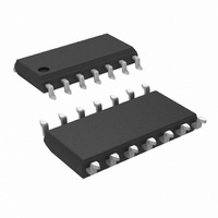
IC LINE RCVR QUAD CMOS 14-SOIC
Manufacturer
National Semiconductor
Type
Receiverr
Datasheet
1.DS14C89AMNOPB.pdf
(5 pages)
Specifications of DS14C89AM/NOPB
Number Of Drivers/receivers
0/4
Protocol
RS232
Voltage - Supply
5V, 12V
Mounting Type
Surface Mount
Package / Case
14-SOIC (3.9mm Width), 14-SOL
Interface Circuit Standard 1
EIA/TIA-232-E/V.28
Number Of Receivers
4
Number Of Transmitters
Not Required
Number Of Transceivers
Not Required
Data Transmission Topology
Point-to-Point
Receiver Signal Type
Single-Ended
Transmitter Signal Type
Not Required
Single Supply Voltage (typ)
5V
Single Supply Voltage (min)
4.5V
Single Supply Voltage (max)
5.5V
Dual Supply Voltage (typ)
Not RequiredV
Dual Supply Voltage (min)
Not RequiredV
Dual Supply Voltage (max)
Not RequiredV
Supply Current
0.9mA
Power Supply Requirement
Single
Operating Temp Range
0C to 75C
Operating Temperature Classification
Commercial
Mounting
Surface Mount
Pin Count
14
Package Type
SOIC N
Lead Free Status / RoHS Status
Lead free / RoHS Compliant
Other names
*DS14C89AM
*DS14C89AM/NOPB
DS14C89AM
*DS14C89AM/NOPB
DS14C89AM


www.national.com
t
t
t
t
t
t
Symbol
PLH
PHL
SK
r
f
nw
V
V
V
I
V
V
I
IN
CC
Absolute Maximum Ratings
If Military/Aerospace specified devices are required,
please contact the National Semiconductor Sales Office/
Distributors for availability and specifications.
Electrical Characteristics
AC Electrical Characteristics
Over recommended operating conditions, unless otherwise specified, C
Symbol
Note 1: “Absolute Maximum Ratings” are those values beyond which the safety of the device cannot be guaranteed. They are not meant to imply that the devices
should be operated at these limits. The tables of “Electrical Characteristics” specify conditions for device operation.
Note 2: Derate N Package 12.1 mW/˚C, and M Package 8.5 mW/˚C above +25˚C.
Note 3: AC input waveforms for test purposes: t
Note 4: Under the power-off supply conditions it is assumed that the power supply potential drops to zero (0V) and is replaced by a low impedance or short circuit
to ground.
Over recommended operating conditions, unless otherwise specified
TH
TL
HY
OH
OL
V
Input Voltage
Receiver Output Voltage
Junction Temperature
Continuous Power Dissipation
Lead Temp.
CC
N Package
M Package
Input High Threshold
Input Low Threshold
Typical Input Hysteresis
Input Current
Output High Voltage
Output Low Voltage
Supply Current
Propagation Delay Low to High
Propagation Delay High to Low
Typical Propagation Delay Skew
Output Rise TIme
Output Fall Time
Pulse Width assumed to be Noise
Parameter
Parameter
@
+25˚C (Note 2)
r
V
V
V
V
V
V
V
V
V
V
(max)
I
No Load, V
= t
OUT
(V
IN
IN
IN
IN
IN
IN
IN
IN
IN
IN
−30V to +30V
f
CC
= 200 ns, V
= +25V
= −25V
= +3V
= −3V
= +15V
= −15V
= +3V
= −3V
= V
= V
GND−0.3V
= +3.2 mA
) +0.3V to
1513 mW
1063 mW
TL
TH
(Note 1)
+150˚C
(Note 3)
(min)
+6V
IN
IH
= 2.7V or 0.5V
Input Pulse Width ≥ 10 µs
Input Pulse Width ≥ 10 µs
= +3V, V
Conditions
V
V
(Note 4)
I
I
OUT
OUT
L
CC
CC
= −3V, f = 20 KHz.
2
ConditIons
= +4.5V to +5.5V
= 0V (Power-Off)
= −3.2 mA
= −20µA
Recommended Operating
Conditions
I
Storage Temp. Range
ESD Rating ≥ 1.8 kV, Typically ≥ 2 kV
(HMB, 1.5 kΩ, 100 pF)
V
Operating Free Air Temp. (T
= 50 pF
CC
(Soldering 4 seconds)
DS14C89A
(GND = 0V)
Min
−0.43
−2.14
−0.43
−3.6
0.43
2.14
0.43
Min
1.3
0.5
3.6
2.8
3.5
+4.5
Min
0
Typ
400
3.5
3.2
A
40
40
)
0.15
Typ
1.0
4.0
4.7
0.5
Max
+5.5
+75
−65˚C to +150˚C
Max
300
300
6.5
6.5
1.0
Max
−8.3
−1.0
−5.0
−1.0
900
2.7
1.9
8.3
1.0
5.0
1.0
0.4
Units
+260˚C
˚C
V
Units
Units
µs
µs
ns
ns
ns
µs
mA
mA
mA
mA
mA
mA
mA
mA
µA
V
V
V
V
V
V
Related parts for DS14C89AM/NOPB
Image
Part Number
Description
Manufacturer
Datasheet
Request
R

Part Number:
Description:
IC, RS-232 RECEIVER, 5.5V, NSOIC-14
Manufacturer:
National Semiconductor
Datasheet:

Part Number:
Description:
National Semiconductor [8-Bit D/A Converter]
Manufacturer:
National Semiconductor
Datasheet:
Part Number:
Description:
National Semiconductor [Media Coprocessor]
Manufacturer:
National Semiconductor
Datasheet:
Part Number:
Description:
Digitally Controlled Tone and Volume Circuit with Stereo Audio Power Amplifier, Microphone Preamp Stage and National 3D Sound
Manufacturer:
National Semiconductor
Datasheet:
Part Number:
Description:
Digitally Controlled Tone and Volume Circuit with Stereo Audio Power Amplifier, Microphone Preamp Stage and National 3D Sound
Manufacturer:
National Semiconductor
Datasheet:
Part Number:
Description:
AC97 Rev 2 Codec with Sample Rate Conversion and National 3D Sound
Manufacturer:
National Semiconductor
Part Number:
Description:
Manufacturer:
National Semiconductor
Datasheet:
Part Number:
Description:
Manufacturer:
National Semiconductor
Datasheet:
Part Number:
Description:
General Purpose, Low Voltage, Low Power, Rail-to-Rail Output Operational Amplifiers
Manufacturer:
National Semiconductor
Datasheet:
Part Number:
Description:
8-bit 20 MSPS flash A/D converter.
Manufacturer:
National Semiconductor
Datasheet:
Part Number:
Description:
Low Noise Quad Operational Amplifier
Manufacturer:
National Semiconductor
Datasheet:
Part Number:
Description:
Quad Differential Line Receivers
Manufacturer:
National Semiconductor
Datasheet:
Part Number:
Description:
Quad High Speed Trapezoidal? Bus Transceiver
Manufacturer:
National Semiconductor
Datasheet:
Part Number:
Description:
Dual Line Receiver
Manufacturer:
National Semiconductor
Datasheet: