ADM2209EARU Analog Devices Inc, ADM2209EARU Datasheet - Page 2
ADM2209EARU
Manufacturer Part Number
ADM2209EARU
Description
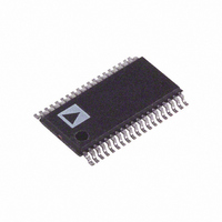
IC TXRX6/10 RS-232 12V 38TSSOP
Manufacturer
Analog Devices Inc
Type
Transceiverr
Datasheet
1.ADM2209EARUZ.pdf
(12 pages)
Specifications of ADM2209EARU
Rohs Status
RoHS non-compliant
Number Of Drivers/receivers
6/10
Protocol
RS232
Voltage - Supply
10.8 V ~ 13.2 V
Mounting Type
Surface Mount
Package / Case
38-TSSOP
Available stocks
Company
Part Number
Manufacturer
Quantity
Price

Part Number:
ADM2209EARU
Manufacturer:
ADI/亚德诺
Quantity:
20 000
Part Number:
ADM2209EARUD
Manufacturer:
ADI/亚德诺
Quantity:
20 000
Part Number:
ADM2209EARUZ
Manufacturer:
ADI/亚德诺
Quantity:
20 000
Company:
Part Number:
ADM2209EARUZ-REEL7
Manufacturer:
BROADCOM
Quantity:
145
Part Number:
ADM2209EARUZ-REEL7
Manufacturer:
ADI/亚德诺
Quantity:
20 000


ADM2209E–SPECIFICATIONS
Parameter
OPERATING CONDITIONS
TRANSMITTER (DRIVER) CMOS INPUTS
TRANSMITTER (DRIVER) EIA-232 OUTPUTS
RECEIVER EIA-232 INPUTS
RECEIVER OUTPUTS
DRIVER SWITCHING CHARACTERISTICS
RECEIVER SWITCHING CHARACTERISTICS
ESD AND EMC
NOTES
1
2
3
4
5
Specifications subject to change without notice.
Refer to typical curves. Driver output slew rate is measured from the +3.0 V to the –3.0 V level on the output waveform. Slew rate is determined by load capacitance.
All typicals are given for V
Current into device pins is defined as positive. Current out-of-device pins is defined as negative. All voltages are referred to ground unless otherwise specified. For
current, minimum and maximum values are specified as an absolute value and the sign is used to indicate direction. For voltage logic levels, the more positive value is
designated as maximum. For example, if –6 V is a maximum, the typical value (–6.8 V) is more negative.
Only one driver output shorted at a time.
If receiver inputs are unconnected, receiver output is a logic high.
Operating Voltage Range, V
Standby Voltage Range, V
V
V
Input Pull-Up Current
High Level Input Voltage, V
Low Level Input Voltage, V
Output Voltage Swing
Output Short-Circuit Current, I
Output Resistance
Input Voltage Range
Input Low Threshold, V
Input High Threshold, V
Input Hysteresis
Input Resistance, R
High Level Output Voltage, V
Low Level Output Voltage, V
Output Leakage Current (Except R5A, R5B)
Maximum Data Rate
Propagation Delay, High to Low, T
Propagation Delay, Low to High, T
Transition Region Slew Rate
Transition Region Slew Rate (5 V)
Maximum Data Rate
Propagation Delay, R1–R4
Propagation Delay, R5
Output Rise Time, t
Output Fall Time, t
ESD Protection (I-O Pins)
ESD Protection
EFT Protection (I-O Pins)
EMI Immunity
DD
STBY
Power Supply Current
Supply Current
(All Other Pins)
DD
IN
f
r
= +12 V, V
4
TL
TH
STBY
2
INL
DD
INH
OL
OH
STBY
OS
= 5 V, T
PHL
PLH
A
= +25 C.
5
Min Typ
+10.8 +12 +13.2 V
+3.15
2.1
300
–15
0.4
3
2.4
460
460
920
6
4
920
460
5.0
5
(V
specifications T
100 200
10
1.45
1.7
0.25
5
0.2
0.05
1
1
16
16
0.4
1
30
30
10
DD
9.0
15
15
15
8
2.5
2
= 10.8 V to 13.2 V, V
–2–
1
Max
+5.5
5
25
0.4
+15
2.4
7
0.4
0.75
2
30
5
MIN
V
mA
V
V
V
mA
V
V
k
V
V
kbps
kbps
kbps
kV
kV
kV
kV
kV
Units
V
V
kbps
V/ s
V/ s
kbps
ns
ns
V/m
A
A
A
s
s
s
s
to T
MAX
STBY
unless otherwise noted.)
Test Conditions/Comments
No Load, All Driver Inputs at 0.8 V or 2 V,
All Receiver Inputs at +15 V or –15 V
No Load, All Tx IN at V
Transmitter Input at GND
All Transmitter Outputs Loaded with 3 k to GND
V
V
V
I
I
V
R
R
T
R
V
R
R
R
R
V
to –3 V or Vice Versa
C
C
C
C
Figures 3 and 4
Human Body Model
IEC1000-4-2 Air Discharge
IEC1000-4-2 Contact Discharge
Human Body Model, MIL-STD-883B
IEC1000-4-4
IEC1000-4-3
OH
OL
O
DD
IN
DD
L
L
L
STBY
L
L
L
L
STBY
A
L
L
L
L
= 3.3 V
= 3 k to 7 k , C
= 3 k to 7 k , C
= 3 k to 7 k , C
= 3 k , C
= 3 k , C
= 3 k to 7 k , C
= 3 k to 7 k , C
= 0 V, V
= 0 C to +85 C, 5 V
= 150 pF, V
= 150 pF
= 150 pF
= 150 pF
= +1.6 mA
= 15 V
= –40 A
= 0 V, V
= 0 V
= 5 V
= 5 V
IN
5% or 5 V
L
L
STBY
= 0.8 V
5%, V
= 1000 pF (Figures 1 and 2)
= 1000 pF (Figures 1 and 2)
10% Only. Measured from +3 V
STBY
= 0 V, V
= 5 V
DD
L
L
L
L
L
3
= 50 pF to 470 pF
= 50 pF to 1000 pF,
= 50 pF to 470 pF,
= 50 pF to 470 pF
= 50 pF to 1000 pF,
= 12 V
10%, C1 = C2 = 0.1 F. All
STBY
IN
10% Only
5% Only
= 2 V
or Open
5%
REV. 0
Related parts for ADM2209EARU
Image
Part Number
Description
Manufacturer
Datasheet
Request
R


Part Number:
Description:
±1.7g Dual-Axis IMEMS Accelerometer Evaluation Board
Manufacturer:
Analog Devices Inc
Datasheet:

Part Number:
Description:
Inertial Sensor Evaluation System
Manufacturer:
Analog Devices Inc
Datasheet:
Part Number:
Description:
Manufacturer:
Analog Devices Inc
Datasheet:
Part Number:
Description:
Manufacturer:
Analog Devices Inc
Datasheet:
Part Number:
Description:
Manufacturer:
Analog Devices Inc
Datasheet:
Part Number:
Description:
Manufacturer:
Analog Devices Inc
Datasheet:
Part Number:
Description:
Manufacturer:
Analog Devices Inc
Datasheet:
Part Number:
Description:
Manufacturer:
Analog Devices Inc
Datasheet:
Part Number:
Description:
Manufacturer:
Analog Devices Inc
Datasheet:
Part Number:
Description:
Manufacturer:
Analog Devices Inc
Datasheet:
Part Number:
Description:
Manufacturer:
Analog Devices Inc
Datasheet:
Part Number:
Description:
Manufacturer:
Analog Devices Inc
Datasheet: