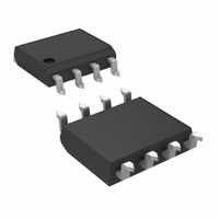
DS92LV010ATMX/NOPB National Semiconductor, DS92LV010ATMX/NOPB Datasheet

DS92LV010ATMX/NOPB
Specifications of DS92LV010ATMX/NOPB
*DS92LV010ATMX/NOPB
DS92LV010ATMX
Available stocks
Related parts for DS92LV010ATMX/NOPB
DS92LV010ATMX/NOPB Summary of contents
Page 1
... The receiver threshold is ±100mV over a ±1V common mode range and translates the low voltage differential levels to stan- dard (CMOS/TTL) levels. Connection Diagram Block Diagram TRI-STATE ® registered trademark of National Semiconductor Corporation. © 2007 National Semiconductor Corporation Features ■ Bus LVDS Signaling (BLVDS) ■ Designed for Double Termination Applications ■ ...
Page 2
... Absolute Maximum Ratings If Military/Aerospace specified devices are required, please contact the National Semiconductor Sales Office/ Distributors for availability and specifications. Supply Voltage ( Enable Input Voltage (DE, −0. RE) Driver Input Voltage (DIN) −0. Receiver Output Voltage (R ) −0. OUT Bus Pin Voltage (DO/RI±) Driver Short Circuit Current ESD (HBM 1.5 kΩ ...
Page 3
DC Electrical Characteristics T = −40°C to +85°C unless otherwise noted Symbol Parameter V Output Differential Voltage OD ΔV V Magnitude Change Offset Voltage OS ΔV Offset Magnitude Change OS I Output Short Circuit ...
Page 4
Symbol Parameter t Disable Time High to Z PHZ t Disable Time Low to Z PLZ t Enable Time Z to High PZH t Enable Time Z to Low PZL DIFFERENTIAL RECEIVER TIMING REQUIREMENTS t Differential Prop. Delay High to ...
Page 5
Test Circuits and Timing Waveforms FIGURE 2. Differential Driver Propagation Delay and Transition Time Test Circuit FIGURE 3. Differential Driver Propagation Delay and Transition Time Waveforms FIGURE 1. Differential Driver DC Test Circuit 5 10005203 10005204 10005205 www.national.com ...
Page 6
FIGURE 6. Receiver Propagation Delay and Transition Time Test Circuit FIGURE 7. Receiver Propagation Delay and Transition Time Waveforms www.national.com FIGURE 4. Driver TRI-STATE Delay Test Circuit FIGURE 5. Driver TRI-STATE Delay Waveforms 6 10005206 10005207 10005208 10005209 ...
Page 7
FIGURE 8. Receiver TRI-STATE Delay Test Circuit FIGURE 9. Receiver TRI-STATE Delay Waveforms TRI-STATE Delay Waveforms Typical Bus Application Configurations Bi-Directional Half-Duplex Point-to-Point Applications Multi-Point Bus Applications 7 10005210 10005211 10005212 10005213 www.national.com ...
Page 8
Application Information There are a few common practices which should be implied when designing PCB for BLVDS signaling. Recommended practices are: • Use at least 4 layer PCB board (BLVDS signals, ground, power and TTL signals). • Keep drivers and ...
Page 9
Physical Dimensions inches (millimeters) unless otherwise noted Order Number DS92LV010ATM See NS Package Number M08A 9 www.national.com ...
Page 10
... For more National Semiconductor product information and proven design tools, visit the following Web sites at: Products Amplifiers www.national.com/amplifiers Audio www.national.com/audio Clock Conditioners www.national.com/timing Data Converters www.national.com/adc Displays www.national.com/displays Ethernet www.national.com/ethernet Interface www.national.com/interface LVDS www.national.com/lvds Power Management www.national.com/power Switching Regulators www.national.com/switchers LDOs www ...


