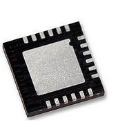
ATA6831-PISW Atmel, ATA6831-PISW Datasheet - Page 10

ATA6831-PISW
Manufacturer Part Number
ATA6831-PISW
Description
MOSFET & Power Driver ICs Triple Half-Bridge Driver
Manufacturer
Atmel
Type
High Side/Low Sider
Datasheet
1.ATA6831N-PIQW.pdf
(17 pages)
Specifications of ATA6831-PISW
Product
Half-Bridge Drivers
Rise Time
100 ns
Fall Time
100 ns
Supply Current
6 mA
Maximum Operating Temperature
+ 150 C
Mounting Style
SMD/SMT
Package / Case
QFN-18
Bridge Type
Half Bridge
Minimum Operating Temperature
- 40 C
Number Of Drivers
3
Number Of Outputs
6
Lead Free Status / Rohs Status
Lead free / RoHS Compliant
8. Electrical Characteristics (Continued)
7.5V < V
10
*) Type means: A = 100% tested, B = 100% correlation tested, C = Characterized on samples, D = Design parameter
Notes:
4.12a
4.10
4.11
4.12
No.
3.6
3.7
3.8
4.1
4.2
4.3
4.4
4.5
4.6
4.7
4.8
4.9
4
VS
1. Delay time between rising edge of input signal at pin CS after data transmission and switch on/off output stages to 90% of
2. Delay time between rising/falling edge of input signal at pin PWM and switch on/off output stages to 90% of final level.
3. Difference between switch-on and switch-off delay time of input signal at pin PWM to output stages in PWM mode.
Parameters
Thermal shutdown
hysteresis
Ratio thermal shutdown
off/thermal prewarning
set
Ratio thermal shutdown
on/thermal prewarning
reset
Output Specification (OUT1 to OUT3)
On resistance
High-side output
leakage current
Low-side output
leakage current
High-side switch
reverse diode forward
voltage
Low-side switch reverse
diode forward voltage
High-side overcurrent
limitation and shutdown
threshold
Low-side overcurrent
limitation and shutdown
threshold
High-side overcurrent
limitation and shutdown
threshold
Low-side overcurrent
limitation and shutdown
threshold
Overcurrent shutdown
delay time
High-side open load
detection current
High-side open load
detection threshold
level
Atmel ATA6831
< 40V; 4.75V < V
final level. Device not in standby for t > 1ms.
VCC
< 5.25V; INH = High; –40°C < T
I
I
V
output stages off
V
output stages off
I
I
7.5V < V
7.5V < V
20V < V
20V < V
Input register bit 13
(OLD) = low, output off
V
Input register bit 13
(OLD) = low, output off
V
Test Conditions
Out1-3
Out1-3
Out
Out 1-3 L
Out 1-3 H
Out 1-3 L
VS
VS
= 1.5A
= 13V, V
= 13V, I
= –0.9A
= –0.9A
= –1.5A
VS
VS
= V
= 0V
VS
VS
< 40V
< 40V
< 20V
< 20V
Out1-3
VS,
Out 1-3
,
= 0mA
= 0V
2, 12,
2, 12,
2, 12,
2, 12,
2, 12,
2, 12,
2, 12,
2, 12,
2, 12,
2, 12,
2, 12,
2, 12,
Pin
15
15
15
15
15
15
15
15
15
15
15
15
j
< 150°C; unless otherwise specified, all values refer to GND pins.
V
V
Out1-3_OLD_HTh
Out1-3
T
T
R
R
Symbol
T
T
V
T
I
I
j switch off/
j switch on/
I
DSon1-3H
jPW reset
DSon1-3L
Out1-3H
I
I
I
I
Out1-3H
Out1-3L
j switch off
Out1-3L
Out1-3
Out1-3
Out1-3
Out1-3
jPW set
t
dSd
– V
VS
V
3.5V
Min.
1.05
1.05
–1.7
–2.0
–15
1.0
1.0
10
VS
1
2
–
V
2.5V
Typ.
–1.3
–1.3
1.2
1.2
1.3
2.5
1.3
15
VS
–
V
VS
Max.
–1.0
–1.0
300
1.5
1.5
2.0
1.7
40
2
4
– 1V
Unit
4908I–AUTO–01/11
mA
µA
µA
µs
K
V
V
A
A
A
A
V
Type*
B
B
B
A
A
A
A
A
A
A
A
A
A
A
A
A


