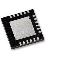
ATA6831-PISW Atmel, ATA6831-PISW Datasheet - Page 7

ATA6831-PISW
Manufacturer Part Number
ATA6831-PISW
Description
MOSFET & Power Driver ICs Triple Half-Bridge Driver
Manufacturer
Atmel
Type
High Side/Low Sider
Datasheet
1.ATA6831N-PIQW.pdf
(17 pages)
Specifications of ATA6831-PISW
Product
Half-Bridge Drivers
Rise Time
100 ns
Fall Time
100 ns
Supply Current
6 mA
Maximum Operating Temperature
+ 150 C
Mounting Style
SMD/SMT
Package / Case
QFN-18
Bridge Type
Half Bridge
Minimum Operating Temperature
- 40 C
Number Of Drivers
3
Number Of Outputs
6
Lead Free Status / Rohs Status
Lead free / RoHS Compliant
3.4
3.5
3.6
3.7
4908I–AUTO–01/11
Overtemperature Protection
Short-circuit Protection
Inhibit
PWM Mode
If the junction temperature of one or more output stages exceeds the thermal prewarning thresh-
old, T
temperature falls below the thermal prewarning threshold, T
bit can be read without transferring a complete 16-bit data word. The status of TP is available at
pin DO with the falling edge of CS. After the microcontroller has read this information, CS is set
high and the data transfer is interrupted without affecting the status of input and output registers.
If the junction temperature of an output stage exceeds the thermal shutdown threshold, T
the affected output is disabled and the corresponding bit in the output register is set to low. Addi-
tionally, the overload detection bit (OVL) in the output register is set. The output can be enabled
again when the temperature falls below the thermal shutdown threshold, T
bit in the input register is set to high. The hysteresis of thermal prewarning and shutdown thresh-
old avoids oscillations.
The output currents are limited by a current regulator. Overcurrent detection is activated by
writing a high to the overcurrent shutdown bit (OCS) bit in the input register. When the current in
an output stage exceeds the overcurrent limitation and shut-down threshold, it is switched off,
following a delay time (t
status bit in the output register is set to low. For OCS = low, the overcurrent shutdown is inactive
and the OVL bit is not set by an overcurrent. By writing a high to the SRR bit in the input register
the OVL bit is reset and the disabled outputs are enabled.
The SI bit in the input register has to be set to zero to inhibit the Atmel ATA6831.
In this state, all output stages are then turned off but the serial interface remains active. The
current consumption is reduced to less than 2µA at pin VS and less than 100µA at pin VCC. The
output stages can be reactivated by setting bit SI to “1”.
The common input for all six outputs is pin PWM
which are controlled by PWM, is done by input data register PLx or PHx. In addition to the PWM
input register, the corresponding input registers HSx and LSs have to be set.
Switching the high side outputs is possible up to 25kHz, low side switches up to 8kHz.
Figure 3-3.
jPW set
Bit PLx/PHx
, the temperature prewarning bit (TP) in the output register is set. When the
Output Control by PWM
dSd
Pin PWM
Bit LSx/HSx
). The over-load detection bit (OVL) is set and the corresponding
(Figure
3-3). The selection of the outputs,
jPW reset
Atmel ATA6831
, the bit TP is reset. The TP
Pin OUTx
jswitch on
, and the SRR
jswitch off
7
,


